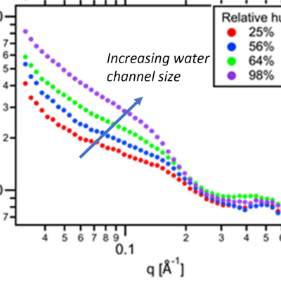
LLNL researchers have developed a method to enhance the performance of polyelectrolyte membranes by using a humidity-controlled crosslinking process which can be applied to precisely adjust the water channels of the membrane.
Image

LLNL researchers has developed designs to augment WBG/UWBG-based OALVs to improve their power handling capability under CW operational environments. These designs include:
Image

CMI—a DOE Energy Innovation Hub—is a public/private partnership led by the Ames Laboratory that brings together the best and brightest research minds from universities, national laboratories (including LLNL), and the private sector to find innovative technology solutions to make better use of materials critical to the success of clean energy technologies as well as develop resilient and secure…
Image
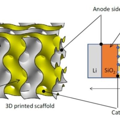
LLNL researchers have developed a new 3D printable lithium-air battery that uses a novel thin solid state ceramic electrolyte. LLNL’s invention overcomes the combined challenges of low power density and low cycle life in previously designed lithium-air batteries by using solid state electrolytes to achieve stability and multiscale structuring of the electrolyte to achieve low interfacial…
Image

Design and construction of a photoconductive switch requires a diamond photoconductor illuminated by light of a certain excitation wavelength. The diamond material is specifically doped with substitutional nitrogen, which act as a source of electrons. The device architecture allows maximum light entering the aperture. The top and bottom electrodes are made of ultra wide band gap (UWBG)…
Image

The approach is to use a custom-designed frustrum and attach it to the optical fiber that connects to the PCSS. Light from the fiber enters the frustrum, spreads out, and enters the PCSS. Any unabsorbed light re-enters the frustrum and, because of its geometry, reflects back into the PCSS itself with only a negligible fraction escaping from the fiber. The shape of the novel frustrum is…
Image

LLNL’s Optically-based Interstory Drift Meter System provides a means to accurately measure the dynamic interstory drift of a vibrating building (or other structure) during earthquake shaking. This technology addresses many of the shortcomings associated with traditional strong motion accelerometer based building monitoring.
LLNL’s discrete diode position sensitive device is a newly…
Image

The Optical Transconductance Varistor (OTV, formerly Opticondistor) overcomes depletion region voltage limitations by optically exciting wide bandgap materials in a compact package. A 100μm thick crystal could have the capability approaching 40kV and would replace numerous equivalent junction devices. Thus, unlike present junction transistors or diodes, this wide bandgap device can be stacked…
Image

Nanomaterials that are emerging out of cutting edge nanotechnology research are a key component for an energy revolution. Carbon-based nanomaterials are ushering in the "new carbon age" with carbon nanotubes, nanoporous carbons, and graphene nanosheets that will prove necessary to provide sustainable energy applications that lessen our dependence on fossil fuels.
Carbon aerogels (CAs)…
Image

The invention relates to a measurement method and system for capturing both the amplitude and phase temporal profile of a transient waveform or a selected number of consecutive waveforms having bandwidths of up to about 10 THz in a single shot or in a high repetition rate mode. The invention consists of an optical preprocessor which can then output a time-scaled replica of the input signal to…