

For this method, a Silicon on Insulator (SOI) wafer is used to tailor etch rates and thickness in initial steps of the process. The simple three step process approach is comprised of grayscale lithography, deep reactive-ion etch (DRIE) and liftoff of the SOI wafer. The liftoff process is used to dissolve the insulating layer, thus separating sections of the wafer as individual…
Image
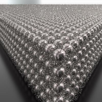
The novel LLNL technique uses electric fields to drive and control assembly. In the literature such methods have heretofore only formed disordered ensembles. This innovative method increases local nanocrystal concentration, initiating nucleation and growth into ordered superlattices. Nanocrystals remain solvated and mobile throughout the process, allowing fast fabrication of ordered…