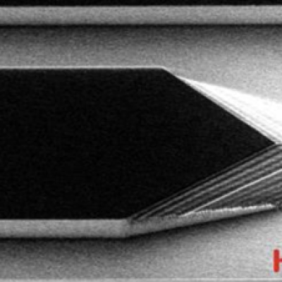
For this method, a Silicon on Insulator (SOI) wafer is used to tailor etch rates and thickness in initial steps of the process. The simple three step process approach is comprised of grayscale lithography, deep reactive-ion etch (DRIE) and liftoff of the SOI wafer. The liftoff process is used to dissolve the insulating layer, thus separating sections of the wafer as individual silicon…
Keywords
- Show all (60)
- Photoconductive Semiconductor Switches (PCSS) (9)
- Imaging Systems (8)
- Semiconductors (6)
- Data Science (5)
- Cybersecurity (4)
- Optical Switches (4)
- Power Electronics (3)
- Sensors (3)
- Simulation (3)
- Computing (2)
- Electric Grid (2)
- Optical Sensors (2)
- Particle Accelerators (2)
- Spectrometers (2)
- Additive Manufacturing (1)
- Precision Engineering (1)
- (-) MEMS Sensors (2)
- (-) Information Technology (1)
Technology Portfolios
Image

LLNL has developed a new active memory data reorganization engine. In the simplest case, data can be reorganized within the memory system to present a new view of the data. The new view may be a subset or a rearrangement of the original data. As an example, an array of structures might be more efficiently accessed by a CPU as a structure of arrays. Active memory can assemble an alternative…
Image

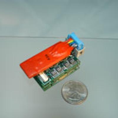
LLNL has developed a compact and low-power cantilever-based sensor array, which has been used to detect various vapor-phase analytes. For further information on the latest developments, see the article "Sniffing the Air with an Electronic Nose."

