
For this method, a Silicon on Insulator (SOI) wafer is used to tailor etch rates and thickness in initial steps of the process. The simple three step process approach is comprised of grayscale lithography, deep reactive-ion etch (DRIE) and liftoff of the SOI wafer. The liftoff process is used to dissolve the insulating layer, thus separating sections of the wafer as individual silicon…
Image
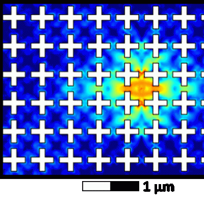
LLNL has developed a method of extending device lifetimes by imprinting into the device a shape that excludes specific vibrational modes, otherwise known as a phononic bandgap. Eliminating these modes prevents one of the primary energy loss pathways in these devices. LLNL’s new method enhances the coherence of superconducting circuits by introducing a phononic bandgap around the system’s…
Image

LLNL’s Optically-based Interstory Drift Meter System provides a means to accurately measure the dynamic interstory drift of a vibrating building (or other structure) during earthquake shaking. This technology addresses many of the shortcomings associated with traditional strong motion accelerometer based building monitoring.
LLNL’s discrete diode position sensitive device is a newly…
Image

The invention relates to a measurement method and system for capturing both the amplitude and phase temporal profile of a transient waveform or a selected number of consecutive waveforms having bandwidths of up to about 10 THz in a single shot or in a high repetition rate mode. The invention consists of an optical preprocessor which can then output a time-scaled replica of the input signal to…