
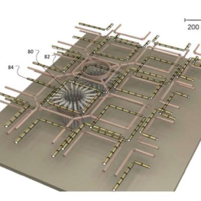
LLNL and its research partners have created miniature ion traps with submicron precision and complex geometries made using 3D printing for fast, high-fidelity and scalable quantum computations. A patent is pending on the technology, with claims covering embodiments for a vertical ion trap, horizontal ion traps and methods of forming the ion traps using advanced manufacturing techniques.
…Image

For this method, a Silicon on Insulator (SOI) wafer is used to tailor etch rates and thickness in initial steps of the process. The simple three step process approach is comprised of grayscale lithography, deep reactive-ion etch (DRIE) and liftoff of the SOI wafer. The liftoff process is used to dissolve the insulating layer, thus separating sections of the wafer as individual…
Image
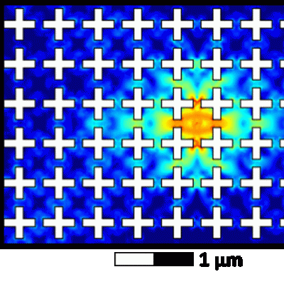
LLNL has developed a method of extending device lifetimes by imprinting into the device a shape that excludes specific vibrational modes, otherwise known as a phononic bandgap. Eliminating these modes prevents one of the primary energy loss pathways in these devices. LLNL’s new method enhances the coherence of superconducting circuits by introducing a phononic bandgap around the system’s…