

LLNL researchers have developed an approach to form silicon carbide (and diamond) nanoneedles using plasma etching that create micro pillars followed by chemical etching of the pillars in forming gas containing hydrogen and nitrogen. Combining these two etching processes allow for fabrication of micro- and nanoneedles that are thinner and sharper than conventionally fabricated needles.
Image
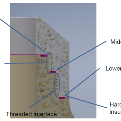
The approach is to build a high voltage insulator consisting of two materials: Poly-Ether-Ether-Ketone (“PEEK”) and Machinable Ceramic (“MACOR”). PEEK has a high stress tolerance but cannot withstand high temperatures, while MACOR has high heat tolerance but is difficult to machine and can be brittle. MACOR is used for the plasma-facing surface, while PEEK will handle the…