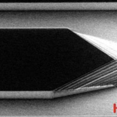
For this method, a Silicon on Insulator (SOI) wafer is used to tailor etch rates and thickness in initial steps of the process. The simple three step process approach is comprised of grayscale lithography, deep reactive-ion etch (DRIE) and liftoff of the SOI wafer. The liftoff process is used to dissolve the insulating layer, thus separating sections of the wafer as individual…
Keywords
- Show all (53)
- Imaging Systems (9)
- Photoconductive Semiconductor Switches (PCSS) (9)
- Semiconductors (7)
- Optical Switches (5)
- Power Electronics (4)
- Additive Manufacturing (2)
- Computing (2)
- Electric Grid (2)
- Sensors (2)
- Spectrometers (2)
- Analysis (1)
- Brain Computer Interface (BCI) (1)
- Compact Space Telescopes (1)
- Instrumentation (1)
- MEMS Sensors (1)
- Particle Accelerators (1)
- Quantum Science (1)
- (-) 3D Electronics (1)
- (-) Optical Sensors (1)
Technology Portfolios
Image

LLNL’s Optically-based Interstory Drift Meter System provides a means to accurately measure the dynamic interstory drift of a vibrating building (or other structure) during earthquake shaking. This technology addresses many of the shortcomings associated with traditional strong motion accelerometer based building monitoring.
LLNL’s discrete diode position sensitive device is a newly…


