

For this method, a Silicon on Insulator (SOI) wafer is used to tailor etch rates and thickness in initial steps of the process. The simple three step process approach is comprised of grayscale lithography, deep reactive-ion etch (DRIE) and liftoff of the SOI wafer. The liftoff process is used to dissolve the insulating layer, thus separating sections of the wafer as individual…
Image
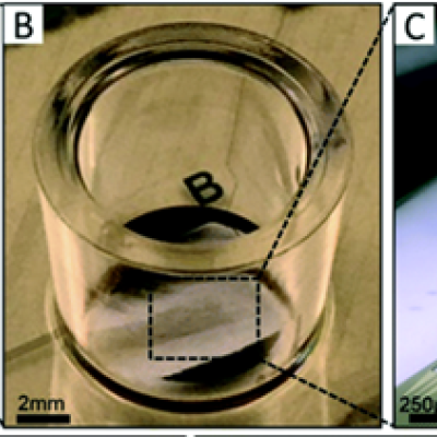
To replicate the physiology and functionality of tissues and organs, LLNL has developed an in vitro device that contains 3D MEAs made from flexible polymeric probes with multiple electrodes along the body of each probe. At the end of each probe body is a specially designed hinge that allows the probe to transition from lying flat to a more upright position when actuated and then…