
For this method, a Silicon on Insulator (SOI) wafer is used to tailor etch rates and thickness in initial steps of the process. The simple three step process approach is comprised of grayscale lithography, deep reactive-ion etch (DRIE) and liftoff of the SOI wafer. The liftoff process is used to dissolve the insulating layer, thus separating sections of the wafer as individual silicon…
Image
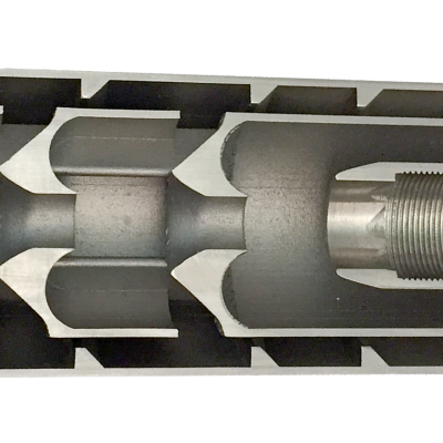
The suppressor has a series of chambers for the propellant to flow through, but unlike all traditional suppressors, the chambers are open, not closed. The propellant is not trapped. It keeps moving. We manage its unimpeded flow through the suppressor. This is the key underlying technology of our suppressor design that enables all the improvements over the 100-year old traditional designs.
Image
Livermore Lab researchers have developed a tunable shaped charge which comprises a cylindrical liner commonly a metal such as copper or molybdenum but almost any solid material can be used and a surround layer of explosive in which the detonation front is constrained to propagate at an angle with respect to the charge axis. The key to the concept is the ability to deposit a surrounding…
Image
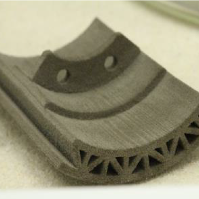
Livermore Lab researchers have developed a method that combines additive manufacturing (AM) with an infill step to render a final component which is energetic. In this case, AM is first used to print a part of the system, and this material can either be inert or energetic on its own. A second material is subsequently added to the structure via a second technique such as casting, melt…