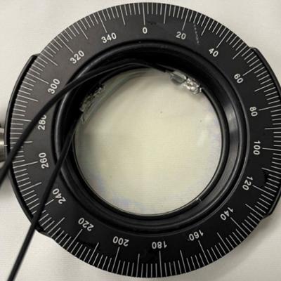
The approach is to use appropriately doped semi-insulating gallium nitride to provide a high damage tolerant photoconductor with high responsivity to various pump wavelength light. Mn, C, or Fe are used as dopants to provide a source of electrons or holes that can be excited. This is combined with the use of dichroic antireflection coating at the GaN/polyimide/liquid crystal…
Keywords
- Show all (240)
- Additive Manufacturing (55)
- Instrumentation (41)
- Synthesis and Processing (21)
- Sensors (14)
- Diagnostics (11)
- Imaging Systems (9)
- Photoconductive Semiconductor Switches (PCSS) (9)
- 3D Printing (8)
- Carbon Utilization (7)
- Electric Grid (7)
- Materials for Energy Products (7)
- Semiconductors (7)
- Substrate Engraved Meta-Surface (SEMS) (7)
- Therapeutics (7)
- Compact Space Telescopes (6)
- Brain Computer Interface (BCI) (5)
- Data Science (5)
- Diode Lasers (5)
- Laser Materials Processing (4)
- (-) Optical Switches (5)
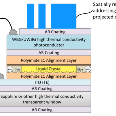
LLNL researchers has developed designs to augment WBG/UWBG-based OALVs to improve their power handling capability under CW operational environments. These designs include:

A set of images generated by multiple passes over the same area can be coherently integrated by this technology developed by LLNL researchers. The primary difficulty with coherently combining different passes is registering the images obtained from each pass, particularly if a pass only partially covers a given area.
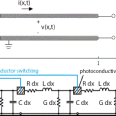
Design and construction of a photoconductive switch requires a diamond photoconductor illuminated by light of a certain excitation wavelength. The diamond material is specifically doped with substitutional nitrogen, which act as a source of electrons. The device architecture allows maximum light entering the aperture. The top and bottom electrodes are made of ultra wide band…
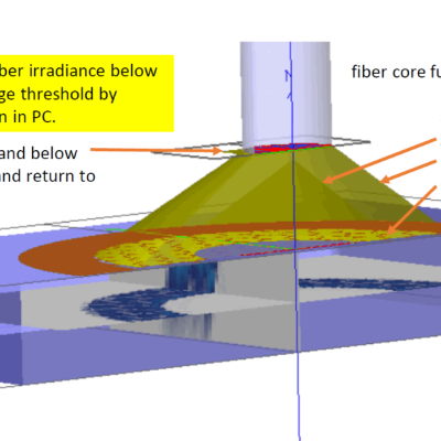
The approach is to use a custom-designed frustrum and attach it to the optical fiber that connects to the PCSS. Light from the fiber enters the frustrum, spreads out, and enters the PCSS. Any unabsorbed light re-enters the frustrum and, because of its geometry, reflects back into the PCSS itself with only a negligible fraction escaping from the fiber. The shape of the novel…
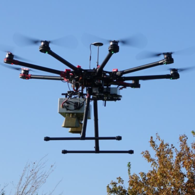
LLNL researchers have developed a lightweight drone-based GPR array that when flown over a surface with laid and/or buried objects could image the field of view and be able to detect targets and discriminate them from clutter. The imaging method employs a modified multi-static architecture to provide the highest signal to noise with the lowest system weight, making it ideal for airborne or…
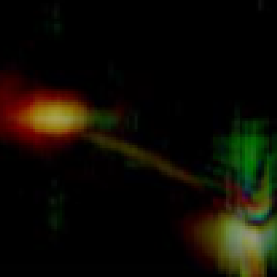
This technology uses three different frequency bands to create intensity maps of returned signals. Signals have traditionally been displayed as raw return data. The intensity of the return is represented by level of brightness. Assignment of a scalar value for intensity is used to determine the brightness of the image. In this technology, each frequency is given a designated…
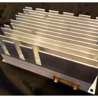
The Optical Transconductance Varistor (OTV, formerly Opticondistor) overcomes depletion region voltage limitations by optically exciting wide bandgap materials in a compact package. A 100μm thick crystal could have the capability approaching 40kV and would replace numerous equivalent junction devices. Thus, unlike present junction transistors or diodes, this wide bandgap device can be stacked…

LLNL has developed a wide band (WB) ground penetrating radar (GPR) technology to detect and image buried objects under a moving vehicle. Efficient and high performance processing algorithms reconstruct images of buried or hidden objects in two or three dimensions under a scanning array. The technology includes a mobile high-performance computing system allowing GPR array sensor data to be…


