LLNL’s invention is a photopolymerizable polymer resin that consists of one or more nitrile-functional based polymers. The resin is formulated for SLA based 3D printing allowing for the production of nitrile-containing polymer components that can then be thermally processed into a conductive, highly graphitic materials. The novelty of the invention lies in (1) the photo-curable nitrile-…
Image

Image
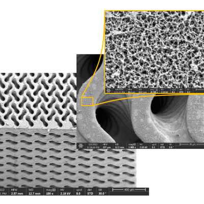
LLNL researchers have developed novel advanced manufactured biomimetic 3D-TPMS (triply periodic minimal surface) membrane architectures such as a 3D gyroid membrane. The membrane is printed using LLNL's nano-porous photoresist technology. LLNL’s 3D-TPMS membranes consist of two independent but interpenetrating macropore flow channel systems that are separated by a thin nano-porous wall. 3D-…
Image
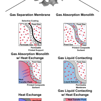
Hierarchical Triply Periodic Minimal Surface Structures For Efficient Two Fluid Flow Reactor Designs
LLNL researchers have devised a set of design principles that facilitates the development of practical TPMS-based two fluid flow reactors.; included in the design are these new concepts:
Image

The approach is to leverage the fact that a momentary “load” equal to the power transmission line impedance, (Z0), during the transient can suppress its propagation. Z(0) is typically a fixed impedance of several hundred ohms based on the geometry of most single wire transmission lines.
So, an isolated self-powered opticondistor (OTV) system may provide an ultrafast method of…
Image

LLNL’s novel approach is to use diamond substrates with the desired donor (nitrogen) and acceptor (boron) impurities. In order to optically activate these deep impurities, the invention requires at least one externally or internally integrated light source. The initial exposure to light can set up the desired conduction current, after which the light source could be turned off. Even with…
Image
![Filled (8,8) (left) and (15,15) (right) CNTs with [EMIM+][BF4- ] using SGTI with the proposed spliced soft-core potential (SSCP) approach](/sites/default/files/styles/scale_exact_400x400_/public/2023-10/Filled%20CNTs%20using%20SGTI.png?itok=Dy0ObN7i)
LLNL researchers have developed a novel simulation methodology using slow growth thermodynamic integration (SGTI) utilizing spliced soft-core interaction potential (SSCP). The approach to filling the molecular enclosures is a nonphysical one. Rather than filling the pores from the open ends this method creates steps in the algorithm that allow molecules to pass through the pore wall and…
Image

Instead of producing individual DSRDs and bonding them, Tunnel DSRD's entire stack structure is grown epitaxially on a n- or p-type silicon wafer, resulting in a novel, “monolithic” stacked DSRD. A tunnel diode is essentially a diode with very highly doped p and n regions such that the reverse breakdown voltage is 200 meV or lower.
Image
By combining 3D printing and dealloying., researchers at LLNL have developed a method for fabricating metal foams with engineered hierarchical architectures consisting of pores at least 3 distinct length scales. LLNL’s method uses direct ink writing (DIW), a 3D printing technique for additive manufacturing to fabricate hierarchical nanoporous metal foams with deterministically controlled 3D…
Image

To overcome limitations with cellular silicone foams, LLNL innovators have developed a new 3D energy absorbing material with tailored/engineered bulk-scale properties. The energy absorbing material has 3D patterned architectures specially designed for specific energy absorbing properties. The combination of LLNL's capabilities in advanced modeling and simulation and the additive…