
For this method, a Silicon on Insulator (SOI) wafer is used to tailor etch rates and thickness in initial steps of the process. The simple three step process approach is comprised of grayscale lithography, deep reactive-ion etch (DRIE) and liftoff of the SOI wafer. The liftoff process is used to dissolve the insulating layer, thus separating sections of the wafer as individual silicon…
Image

Recent advancements in additive manufacturing, also called 3D printing, allow precise placement of materials in three dimensions. LLNL researchers have invented mechanical logic gates based on flexures that can be integrated into the microstructure of a micro-architected material through 3D printing. The logic gates can be combined into circuits allowing complex logic operations to be…
Image
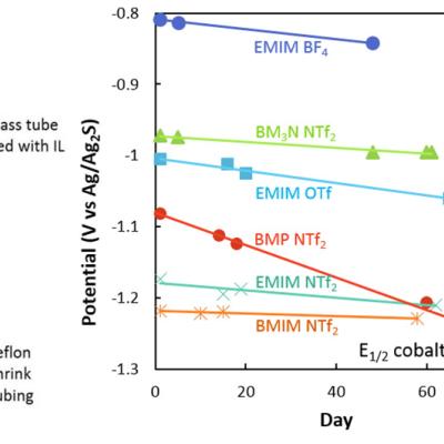
LLNL has developed a reference electrode that is a great improvement on the widely used silver or platinum wire QRE commonly used in electrochemistry in ionic liquids. This new reference electrode, based on a silver-sulfide coated silver wire, exhibits greatly improved stability over a QRE. The stability of our RE approaches that of the Ag/Ag+ RE, but unlike the Ag/Ag+ RE, the RE reported here…