LLNL’s novel approach utilizes a number of techniques to improve reconstruction accuracy:
Image
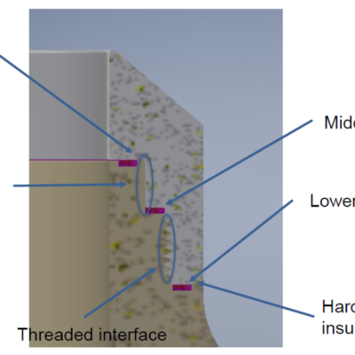
The approach is to build a high voltage insulator consisting of two materials: Poly-Ether-Ether-Ketone (“PEEK”) and Machinable Ceramic (“MACOR”). PEEK has a high stress tolerance but cannot withstand high temperatures, while MACOR has high heat tolerance but is difficult to machine and can be brittle. MACOR is used for the plasma-facing surface, while PEEK will handle the stresses and high…
Image
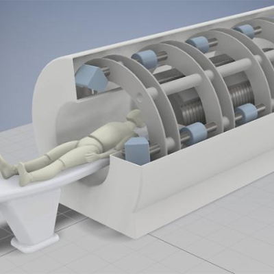
LLNL’s approach is to use their patented Photoconductive Charge Trapping Apparatus (U.S. Patent No. 11,366,401) as the active switch needed to discharge voltage across a vacuum gap in a particle accelerator, like the one described in their other patent (U.S. Patent No.
Image
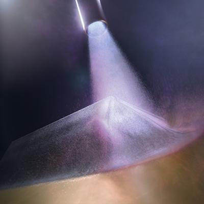
Versatile Cold Spray (VCS) enables deposition of brittle materials, such as thermoelectrics, magnets, and insulators, while retaining their functional properties. Materials can be deposited on substrates or arbitrary shapes with no requirement to match compositions. The VCS system is low cost, easily portable, and easy to use.
VCS has been developed in a collaboration between Lawrence Livermore…
Image
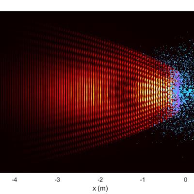
LLNL pioneered the use of tomographic reconstruction to determine the power density of electron beams using profiles of the beam taken at a number of angles. LLNL’s earlier diagnostic consisted of a fixed number of radially oriented sensor slits and required the beam to be circled over them at a fixed known diameter to collect data. The new sensor design incorporates annular slits instead,…