This invention proposes to engineer the current density along the length of a laser diode to overcome the penalty associated with non-uniformity resulting from asymmetry in the gain, photon or carrier density despite having uniform contact. Optimizing the current density profile enables diode lasers to operate with greater power conversion efficiency or operate with equivalent power conversion…
Image

This invention proposes to engineer the temperature dependence of the emission wavelength of LEDs and laser diodes. The approach is to use a strain-inducing coating to counteract the intrinsic temperature coefficient of the emission wavelength of the LED or laser diode device thereby rendering it athermal. This invention avoids additional complexity, size, weight and power dissipation of…
Image

This invention proposes a method to overcome the key limitation of electrically pumped lasers based on AlN, AlGaN, or AlInGaN, namely the lack of suitable shallow donor and acceptor dopants. As the band gap of these materials increases (and the emission wavelength decreases), both electrons and holes require greater thermal energies in order to ionize.
Image

Laser diode lensing effect can be substantially reduced by creating a pattern interface such that the substrate is only attached at the diode mesa. This is achieved by either creating a pattern solder joint and/or pattern substrate.
Image
LLNL researchers have developed a high average power Faraday rotator that is gas-cooled and uniquely designed to dissipate heat uniformly so that it does not build up in the optical component and affect its performance. The Faraday rotator material is sliced into smaller disks like a loaf of bread so that high speed helium gas can flow between the slices. With this highly efficient cooling…
Image

For this method, a Silicon on Insulator (SOI) wafer is used to tailor etch rates and thickness in initial steps of the process. The simple three step process approach is comprised of grayscale lithography, deep reactive-ion etch (DRIE) and liftoff of the SOI wafer. The liftoff process is used to dissolve the insulating layer, thus separating sections of the wafer as individual silicon…
Image
This invention discloses a method to minimize transient variations in the wavelength- and/or pointing-behavior of an optic, without requiring a reduction in its thermal resistance, optical absorption, or operating irradiance. The invention employs a combination of a time-varying heat source and time-varying thermal resistance and/or heat sink temperature to achieve temperature stability of the…
Image
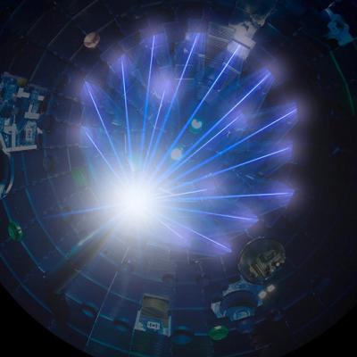
This invention concerns a new type of optic: a transient gas or plasma volume grating produced indirectly by small secondary lasers or directly by nonlinear processes using the primary beams themselves. When used in conjunction with advantageously placed shielding it offers a means of protecting the final optical components of a high-repetition-rate IFE facility. These transmission optics are…
Image
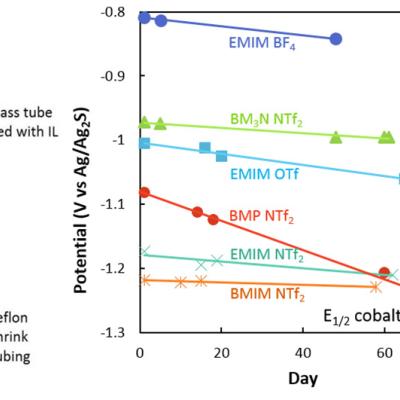
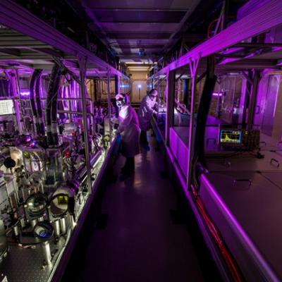
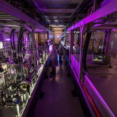
LLNL has developed a reference electrode that is a great improvement on the widely used silver or platinum wire QRE commonly used in electrochemistry in ionic liquids. This new reference electrode, based on a silver-sulfide coated silver wire, exhibits greatly improved stability over a QRE. The stability of our RE approaches that of the Ag/Ag+ RE, but unlike the Ag/Ag+ RE, the RE reported here…
Image

LLNL has developed a compact and low-power cantilever-based sensor array, which has been used to detect various vapor-phase analytes. For further information on the latest developments, see the article "Sniffing the Air with an Electronic Nose."