

LLNL researchers have developed an approach to form silicon carbide (and diamond) nanoneedles using plasma etching that create micro pillars followed by chemical etching of the pillars in forming gas containing hydrogen and nitrogen. Combining these two etching processes allow for fabrication of micro- and nanoneedles that are thinner and sharper than conventionally fabricated needles.
Image

For this method, a Silicon on Insulator (SOI) wafer is used to tailor etch rates and thickness in initial steps of the process. The simple three step process approach is comprised of grayscale lithography, deep reactive-ion etch (DRIE) and liftoff of the SOI wafer. The liftoff process is used to dissolve the insulating layer, thus separating sections of the wafer as individual…
Image
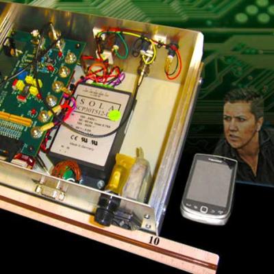
The technology that is available has the capability to inject realistic radiation detection spectra into the amplifier of a radiation detector and produce the all the observables that are available with that radiation detection instrument; count-rate, spectrum, dose rate, etc.
The system uses the capability of LLNL to generate the source output for virtually any source and determine…
Image
Dubbed the "LLNL Chemical Prism", the LLNL system has use wherever there is a need to separate components of a fluid. A few examples include:
- Chemical detection for known and previously unknown chemicals or substances
- Separation of biomolecules from a cellular extract
- Fractionation of a complex mixture of hydrocarbons
- Forensic analysis of…