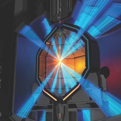
LLNL researchers have developed additive manufactured fuel targets for IFE. They have been successful in using TPL to fabricate low density (down to 60 mg/cm3) and low atomic number (CHO) polymeric foams for potential targets, and some have been tested at the OMEGA Laser Facility. With TPL, LLNL researchers have also been able to fabricate a full fuel capsule with diameter of ~ 5mm or…
Keywords
- Show all (240)
- Additive Manufacturing (55)
- Instrumentation (41)
- Synthesis and Processing (21)
- Sensors (14)
- Diagnostics (11)
- Imaging Systems (9)
- Photoconductive Semiconductor Switches (PCSS) (9)
- 3D Printing (8)
- Carbon Utilization (7)
- Electric Grid (7)
- Materials for Energy Products (7)
- Semiconductors (7)
- Therapeutics (7)
- Compact Space Telescopes (6)
- Brain Computer Interface (BCI) (5)
- Data Science (5)
- Optical Switches (5)
- Laser Materials Processing (4)
- (-) Substrate Engraved Meta-Surface (SEMS) (7)
- (-) Diode Lasers (5)
Technology Portfolios
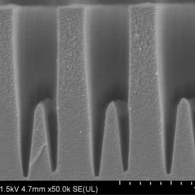
This LLNL invention allows for the fabrication of complex waveplate features and topologies from fused silica, a highly desirable and durable waveplate material. It also is a unique technique for density multiplication and high-fidelity bidirectional deposition, which can create optical components that are generally for entirely new classes of optical materials.
Left Image Caption…
This LLNL invention concerns a method for patterning the index of refraction by fabricating a spatially invariant metasurface, and then apply spatially varied mechanical loading to compress the metasurface features vertically and spread them radially. In doing so, the index of refraction can be re-written on the metasurface, thus enabling index patterning. This process allows rapid 'rewriting…
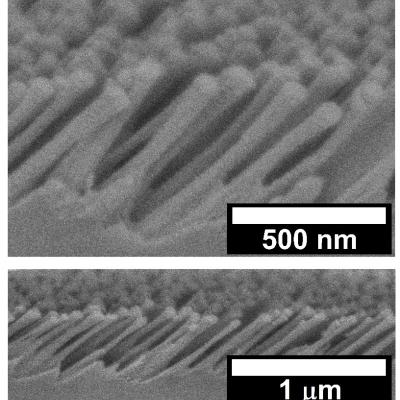
This novel invention specifically enables the fabrication of arbitrarily tailored birefringence characteristics in nano-structured meta-surfaces on non-birefringent substrates (e.g. fused silica). The birefringent nano-structured meta-surface is produced by angled directional reactive ion beam etching through a nano-particle mask. This method enables the simultaneous tailoring of refractive…
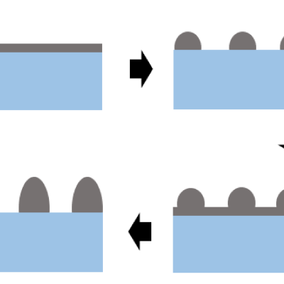
This invention (US Patent No. 11,294,103) is an extension of another LLNL invention, US Patent No. 10,612,145, which utilizes a thin sacrificial metal mask layer deposited on a dielectric substrate (e.g. fused silica) and subsequently nanostructured through a laser generated selective thermal de-wetting process.

This invention proposes to engineer the current density along the length of a laser diode to overcome the penalty associated with non-uniformity resulting from asymmetry in the gain, photon or carrier density despite having uniform contact. Optimizing the current density profile enables diode lasers to operate with greater power conversion efficiency or operate with equivalent power conversion…
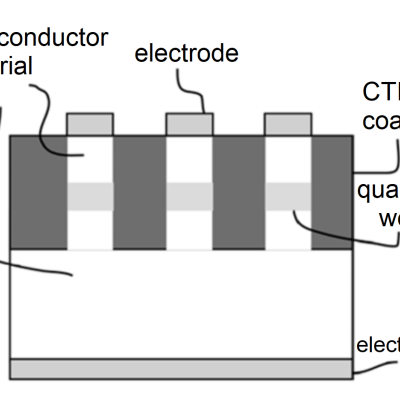
This invention proposes to engineer the temperature dependence of the emission wavelength of LEDs and laser diodes. The approach is to use a strain-inducing coating to counteract the intrinsic temperature coefficient of the emission wavelength of the LED or laser diode device thereby rendering it athermal. This invention avoids additional complexity, size, weight and power dissipation of…
This invention proposes a method to overcome the key limitation of electrically pumped lasers based on AlN, AlGaN, or AlInGaN, namely the lack of suitable shallow donor and acceptor dopants. As the band gap of these materials increases (and the emission wavelength decreases), both electrons and holes require greater thermal energies in order to ionize.

Laser diode lensing effect can be substantially reduced by creating a pattern interface such that the substrate is only attached at the diode mesa. This is achieved by either creating a pattern solder joint and/or pattern substrate.

This invention configures multiple spherical substrate targets to roll independently of one another. The spheres’ rolling motion is deliberately randomized to promote uniform coating while eliminating the interaction (rubbing, sliding) of adjacent spheres that is present in conventional sphere coating designs. The devices’ novel structure features enable the collimation of depositing…
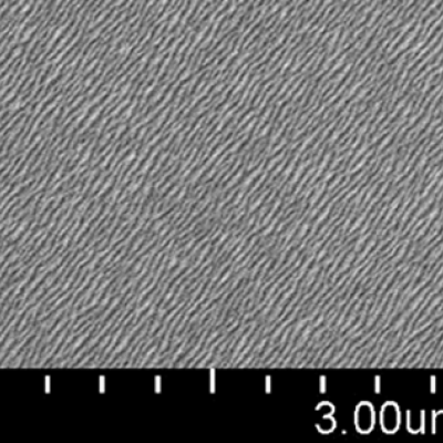
This invention consists of a method of forming nanoscale metal lines to produce a grating-like mask with wide area coverage over the surface of a durable optical material such as fused silica. Subsequent etching processes transfer the metal mask to the underlying substrate forming a birefringent metasurface. This method enables the production of ultrathin waveplates for high power laser…
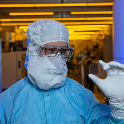
Heat sensitive materials such as piezoelectric and MEMS devices and assemblies, magnetic sensors, nonlinear optical crystals, laser glass or solid-state laser materials, etc. cannot be exposed to excess temperatures which in the context of this invention, means materials that cannot be exposed to temperatures greater than 50°C (122°F). LLNL’s invention describes a low-temperature method of…
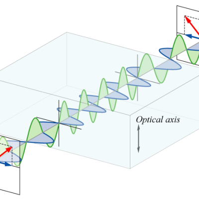
This novel method of producing waveplates from isotropic optical materials (e.g. fused silica) consists of forming a void-dash metasurface using the following process steps:


