
This invention solves a limitation in the current practice of adding hydroxyl functional groups to the aminopolymer through the use of an alternative synthetic approach. The novelty of our approach is to produce new structurally modified relatives of common aminopolymers (PEI and PPI) as well as new functionalized materials in which the hydroxyl groups are tethered to a carbon in the backbone…
Image
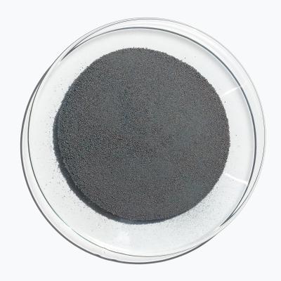
LLNL researchers have developed a Li-Sn-Zn ternary alloy and its method of production. Instead of traditional alloying techniques, the alloy was synthesized using mechanical alloying (high energy ball milling). With high purity elemental powders of lithium, tin and zinc, LLNL researchers were able to prepare Li60Sn20Zn20 as well as Li70Sn20Zn10 nanopowders.
Image

The approach is to leverage the fact that a momentary “load” equal to the power transmission line impedance, (Z0), during the transient can suppress its propagation. Z(0) is typically a fixed impedance of several hundred ohms based on the geometry of most single wire transmission lines.
So, an isolated self-powered opticondistor (OTV) system may provide an ultrafast method of…
Image

LLNL’s novel approach is to use diamond substrates with the desired donor (nitrogen) and acceptor (boron) impurities. In order to optically activate these deep impurities, the invention requires at least one externally or internally integrated light source. The initial exposure to light can set up the desired conduction current, after which the light source could be turned off. Even with…
Image

Instead of producing individual DSRDs and bonding them, Tunnel DSRD's entire stack structure is grown epitaxially on a n- or p-type silicon wafer, resulting in a novel, “monolithic” stacked DSRD. A tunnel diode is essentially a diode with very highly doped p and n regions such that the reverse breakdown voltage is 200 meV or lower.
Image

CMI—a DOE Energy Innovation Hub—is a public/private partnership led by the Ames Laboratory that brings together the best and brightest research minds from universities, national laboratories (including LLNL), and the private sector to find innovative technology solutions to make better use of materials critical to the success of clean energy technologies as well as develop resilient and secure…
Image
This invention describes a multiple nozzle microfluidic unit that allows simultaneous generation streams of multiple layered coaxial liquid jets. Liquids are pumped into the device at a combined flow rate from 100 mL/hr to 10 L/hr. Droplets are created with diameters in the range of 1 µm to 5 mm and can be created with 1-2 shell layers encapsulating fluid. Droplets created from the system can…