
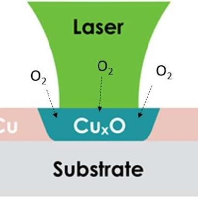
LLNL researchers developed a novel strategy that involves material transformations such as oxidation, nitridation, or carbonization. In one embodiment, copper is heated under ambient conditions resulting in its surface being oxidized and turned into copper oxide, where a new material (e.g., copper oxide) is developed via transformation (e.g., oxidation) without additional addition deposition…
Image
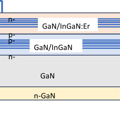
This LLNL invention is a wide bandgap (WBG) or ultra-wide bandgap (UWBG) material comprising a PCSS that is modified, either chemically through alloying and/or mechanically through strain fields, in order to tune the energetic positions of the valence and/or conduction bands and the associated optical transition energies that create and quench the PCSS responsivity.
Image

A thyristor will stay conducting until the current through the device is zero (“current zero”) or perhaps slightly negative. LLNL’s approach is to use the opticondistor (“OTV”) to force this current zero in order to force the device into an “off” state. By combining a light-activated thyristor with an OTV, a noise-immune, high efficiency, high-power switching device can be…
Image

The researchers’ approach leverages the concept that dopants have high diffusivities in Ga2O3; the key lies in the selection of the appropriate dopant. This LLNL invention describes two device types that employ this design:
Image

Design and construction of a photoconductive switch requires a diamond photoconductor illuminated by light of a certain excitation wavelength.
Characteristics of the LLNL-developed switch are as follows:
Image
This invention takes advantage of the high water-solubility of key NIF KDP crystal optics and uses water as an etchant to remove surface defects and improve the laser induced damage threshold. Since pure water etches KDP too fast, this invention is to disperse water as nanosized droplets in a water-in-oil micro-emulsion. While in a stable micro-emulsion form, the surfactant additives prevent…
Image
This invention proposes to use laser induced melting/softening to locally reshape the form of a glass optic. The local glass densification that results induces predictable stresses that through plate deformation mechanics yield a deterministic methodology for arbitrarily reshaping an optic surface figure and wavefront without the need to remove material.
Image

LLNL researchers have invented an ultrafast PCSS to drive a high-power laser diode with arbitrary pulse widths. These devices operate by supplying a high voltage (>10 kV) to one side of the switch. A short pulse of light illuminates the semiconductor, instantly turning it from highly resistive to highly conductive. Ultrawide bandgap (UWBG) semiconductors are used to achieve sub-…
Image

The approach is to leverage the fact that a momentary “load” equal to the power transmission line impedance, (Z0), during the transient can suppress its propagation. Z(0) is typically a fixed impedance of several hundred ohms based on the geometry of most single wire transmission lines.
So, an isolated self-powered opticondistor (OTV) system may provide an ultrafast method of…
Image

LLNL’s novel approach to enable MVDC power systems to operate safely is to develop a wideband gap bulk optical semiconductor switch (WBG BOSS) circuit breaker. For higher power, efficiency and temperature operation, vanadium-doped silicon carbide (V-doped SiC) appears to be the most promising basis for WBG BOSS circuit breaker (other dopants like aluminum, boron and nitrogen may further…
Image
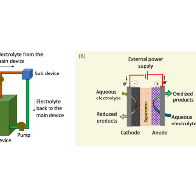
LLNL researchers has developed an approach to mitigate HER on the ‘plating’ electrode, which uses a sub-device as a rebalancing cell to restore electrolyte properties, including pH, conductivity, and capacity across the main device of the flow battery. This sub-device, which may need to be powered externally, has three major physical components: (1) a cathode electrode, (2) an anode…
Image

LLNL has developed a novel methodology for using commercially available automated sensors and actuators which can be deployed at scale in large appliances and plug-in EVs to provide as needed electric grid stabilization capabilities. The approach comprises of a population of voltage relays with a range of setpoints that would gradually reduce load as voltage falls. More severe voltage…
Image

Improving the active material of the Zn anode is critical to improving the practicality of Zn-MnO2 battery technology. LLNL researchers have developed a new category of 3D structured Zn anode using a direct-ink writing (DIW) printing process to create innovative hierarchical architectures. The DIW ink, which is a gel-based mixture composed of zinc metal powder and organic binders, is…
Image
To address many of the aforementioned challenges of manufacturing LIBs and SSBs, LLNL researchers have developed a number of inventions that offer proposed solutions for their components:
Image

U.S. Patent No. 11,555,965 describes LLNL’s invention of “Illumination Frustums” for photoconductive switches to capture and “frustrate” the light from leaving the frustum. LLNL researcher’s latest novel invention, “Twister Oven”, achieves this by encouraging laser light absorption in a photo conductor material. Light enters the oven twisting and reflecting, making near normal…
Image

LLNL researchers faced this challenge by bridging the gap between VEDs and solid-state electronics (SSE). Their approach was to create a hybrid vacuum microelectronic device (VMD) architecture that combines the properties of vacuum as the electronic medium and the compact form factor and manufacturing scalability of semiconductor microelectronic chips.
Image

Design and construction of a photoconductive switch requires a diamond photoconductor illuminated by light of a certain excitation wavelength. The diamond material is specifically doped with substitutional nitrogen, which act as a source of electrons. The device architecture allows maximum light entering the aperture. The top and bottom electrodes are made of ultra wide band…
Image

The approach is to use a custom-designed frustrum and attach it to the optical fiber that connects to the PCSS. Light from the fiber enters the frustrum, spreads out, and enters the PCSS. Any unabsorbed light re-enters the frustrum and, because of its geometry, reflects back into the PCSS itself with only a negligible fraction escaping from the fiber. The shape of the novel…
Image
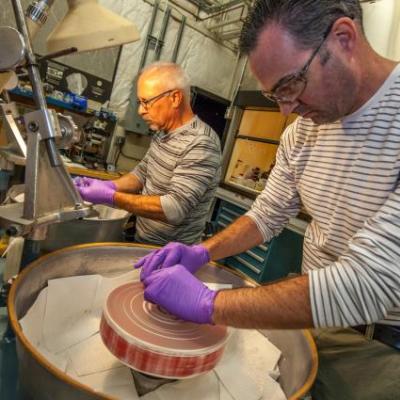
LLNL's Slurry Stabilization Method provides a chemical means of stabilizing a polishing compound in suspension at working concentrations without reducing the rate of material removal. The treated product remains stable for many months in storage.