
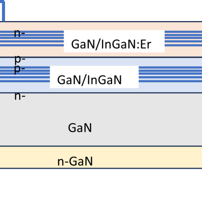
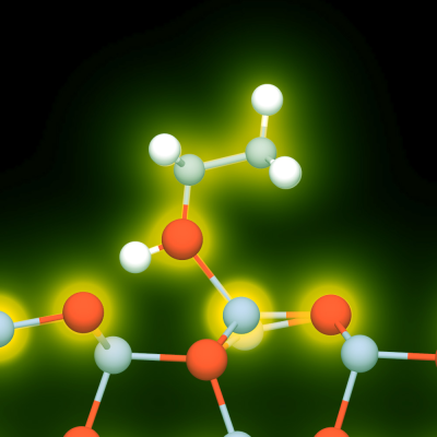
This LLNL invention is a wide bandgap (WBG) or ultra-wide bandgap (UWBG) material comprising a PCSS that is modified, either chemically through alloying and/or mechanically through strain fields, in order to tune the energetic positions of the valence and/or conduction bands and the associated optical transition energies that create and quench the PCSS responsivity.
Image

Powder atomic layer deposition process is used to coat nanopowders of host materials (e.g. yttrium aluminum garnet) with optically active neodymium organometal precursor followed by O2/O3 RF plasma to convert to a single layer of Nd2O3. The process can be repeated to build arbitrarily thick layers with custom doping profiles and followed by post-…
Image
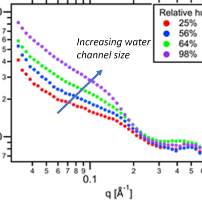
LLNL researchers have developed a method to enhance the performance of polyelectrolyte membranes by using a humidity-controlled crosslinking process which can be applied to precisely adjust the water channels of the membrane.
Image

A thyristor will stay conducting until the current through the device is zero (“current zero”) or perhaps slightly negative. LLNL’s approach is to use the opticondistor (“OTV”) to force this current zero in order to force the device into an “off” state. By combining a light-activated thyristor with an OTV, a noise-immune, high efficiency, high-power switching device can be…
Image

The researchers’ approach leverages the concept that dopants have high diffusivities in Ga2O3; the key lies in the selection of the appropriate dopant. This LLNL invention describes two device types that employ this design:
Image

This invention proposes using a pulse laser configured to generate laser pulses and a controller for controlling operation of the pulse laser. The controller is further configured to control the pulse laser to cause the pulse laser to generate at least one of the laser pulses with a spatiotemporally varying laser fluence over a duration of at least one of the laser pulses. The spatiotemporally…
Image

Design and construction of a photoconductive switch requires a diamond photoconductor illuminated by light of a certain excitation wavelength.
Characteristics of the LLNL-developed switch are as follows:
Image

LLNL researchers have invented an ultrafast PCSS to drive a high-power laser diode with arbitrary pulse widths. These devices operate by supplying a high voltage (>10 kV) to one side of the switch. A short pulse of light illuminates the semiconductor, instantly turning it from highly resistive to highly conductive. Ultrawide bandgap (UWBG) semiconductors are used to achieve sub-…
Image
CMI—a DOE Energy Innovation Hub—is a public/private partnership led by the Ames Laboratory that brings together the best and brightest research minds from universities, national laboratories (including LLNL), and the private sector to find innovative technology solutions to make better use of materials critical to the success of clean energy technologies as well as develop resilient and secure…
Image
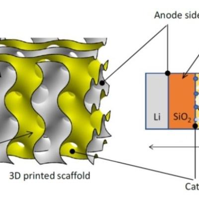
LLNL researchers have developed a new 3D printable lithium-air battery that uses a novel thin solid state ceramic electrolyte. LLNL’s invention overcomes the combined challenges of low power density and low cycle life in previously designed lithium-air batteries by using solid state electrolytes to achieve stability and multiscale structuring of the electrolyte to achieve low…
Image

U.S. Patent No. 11,555,965 describes LLNL’s invention of “Illumination Frustums” for photoconductive switches to capture and “frustrate” the light from leaving the frustum. LLNL researcher’s latest novel invention, “Twister Oven”, achieves this by encouraging laser light absorption in a photo conductor material. Light enters the oven twisting and reflecting, making near normal…
Image

LLNL researchers faced this challenge by bridging the gap between VEDs and solid-state electronics (SSE). Their approach was to create a hybrid vacuum microelectronic device (VMD) architecture that combines the properties of vacuum as the electronic medium and the compact form factor and manufacturing scalability of semiconductor microelectronic chips.
Image

Design and construction of a photoconductive switch requires a diamond photoconductor illuminated by light of a certain excitation wavelength. The diamond material is specifically doped with substitutional nitrogen, which act as a source of electrons. The device architecture allows maximum light entering the aperture. The top and bottom electrodes are made of ultra wide band…
Image

The approach is to use a custom-designed frustrum and attach it to the optical fiber that connects to the PCSS. Light from the fiber enters the frustrum, spreads out, and enters the PCSS. Any unabsorbed light re-enters the frustrum and, because of its geometry, reflects back into the PCSS itself with only a negligible fraction escaping from the fiber. The shape of the novel…
Image

Livermore Lab researchers have developed two new methods for improving the efficiency of laser drilling. The first method is based on multi-pulse laser technology. Two synchronized free-running laser pulses from a tandem-head Nd:YAG laser and a gated CW laser are capable of drilling through 1/8-in-thick stainless-steel targets at a standoff distance of 1 m without gas-assist. The combination of a…
Image

Livermore researchers have developed two novel TiCl4 based non-alkoxide sol-gel approaches for the synthesis of SiO2/TiO2 nanocomposite aerogels. Composite SiO2-TiO2 aerogels were obtained by epoxide-assisted gelation (EAG route) of TiCl4/DMF solution in the presence SiO2 aerogel particles. Additionally, the same TiCl4/DMF solution was employed to prepare SiO2@TiO2 aerogels by a facile one-…
Image
Chemical and biological sensors based on nanowire or nanotube technologies exhibit observable ultrasensitive detection limits due to their unusually large surface-to-volume architecture. This suggests that nanosensors can provide a distinct advantage over conventional designs. This advantage is further enhanced when the nanosensor can harvest its meager power requirements from the surrounding…
Image

The new LLNL technique works by transiently removing and trapping concrete or rock surface material, so that contaminants are confined in a manner that is easy to isolate and remove. Our studies suggest that 10 m2 of surface could be processed per hour. The technique easily scales to more surface/hr.
Image

Nanomaterials that are emerging out of cutting edge nanotechnology research are a key component for an energy revolution. Carbon-based nanomaterials are ushering in the "new carbon age" with carbon nanotubes, nanoporous carbons, and graphene nanosheets that will prove necessary to provide sustainable energy applications that lessen our dependence on fossil fuels.
Carbon aerogels (CAs)…
Image
LLNL has developed novel nanoporous carbon materials for the surface-stress-induced actuator technology. The morphology of these materials has been designed to combine high surface area and mechanical strength. The process allows for the fabrication of large monolithic pieces with low densities and high structural integrity. One actuation technology relies on electrochemically- induced changes…