

LLNL developed a novel SOS diode structure starting with a n-type silicon wafer. On the appropriate sides of the wafer, donor and acceptor dopants with specifically designed and optimized concentration profiles are diffused in the structure. Crucially, an extra n-region is introduced to the structure to address pre-pulses. The result is a SOS diode with an optimized p+/p/n-…
Image

Powder atomic layer deposition process is used to coat nanopowders of host materials (e.g. yttrium aluminum garnet) with optically active neodymium organometal precursor followed by O2/O3 RF plasma to convert to a single layer of Nd2O3. The process can be repeated to build arbitrarily thick layers with custom doping profiles and followed by post-…
Image

This invention proposes using a pulse laser configured to generate laser pulses and a controller for controlling operation of the pulse laser. The controller is further configured to control the pulse laser to cause the pulse laser to generate at least one of the laser pulses with a spatiotemporally varying laser fluence over a duration of at least one of the laser pulses. The spatiotemporally…
Image

The approach is to leverage the fact that a momentary “load” equal to the power transmission line impedance, (Z0), during the transient can suppress its propagation. Z(0) is typically a fixed impedance of several hundred ohms based on the geometry of most single wire transmission lines.
So, an isolated self-powered opticondistor (OTV) system may provide an ultrafast method of…
Image

LLNL’s novel approach is to use diamond substrates with the desired donor (nitrogen) and acceptor (boron) impurities. In order to optically activate these deep impurities, the invention requires at least one externally or internally integrated light source. The initial exposure to light can set up the desired conduction current, after which the light source could be turned…
Image

Instead of producing individual DSRDs and bonding them, Tunnel DSRD's entire stack structure is grown epitaxially on a n- or p-type silicon wafer, resulting in a novel, “monolithic” stacked DSRD. A tunnel diode is essentially a diode with very highly doped p and n regions such that the reverse breakdown voltage is 200 meV or lower.
Image
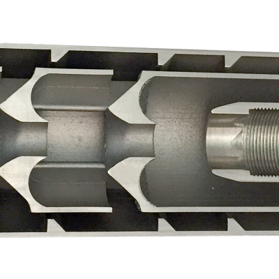
The suppressor has a series of chambers for the propellant to flow through, but unlike all traditional suppressors, the chambers are open, not closed. The propellant is not trapped. It keeps moving. We manage its unimpeded flow through the suppressor. This is the key underlying technology of our suppressor design that enables all the improvements over the 100-year old traditional designs.
Image
Livermore Lab researchers have developed a tunable shaped charge which comprises a cylindrical liner commonly a metal such as copper or molybdenum but almost any solid material can be used and a surround layer of explosive in which the detonation front is constrained to propagate at an angle with respect to the charge axis. The key to the concept is the ability to deposit a surrounding…
Image

Livermore Lab researchers have developed two new methods for improving the efficiency of laser drilling. The first method is based on multi-pulse laser technology. Two synchronized free-running laser pulses from a tandem-head Nd:YAG laser and a gated CW laser are capable of drilling through 1/8-in-thick stainless-steel targets at a standoff distance of 1 m without gas-assist. The combination of a…
Image
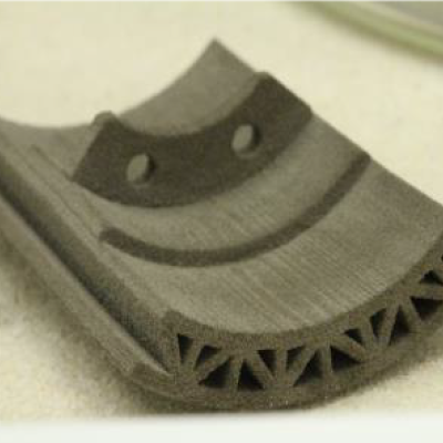
Livermore Lab researchers have developed a method that combines additive manufacturing (AM) with an infill step to render a final component which is energetic. In this case, AM is first used to print a part of the system, and this material can either be inert or energetic on its own. A second material is subsequently added to the structure via a second technique such as casting, melt…
Image

The new LLNL technique works by transiently removing and trapping concrete or rock surface material, so that contaminants are confined in a manner that is easy to isolate and remove. Our studies suggest that 10 m2 of surface could be processed per hour. The technique easily scales to more surface/hr.