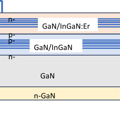
This LLNL invention is a wide bandgap (WBG) or ultra-wide bandgap (UWBG) material comprising a PCSS that is modified, either chemically through alloying and/or mechanically through strain fields, in order to tune the energetic positions of the valence and/or conduction bands and the associated optical transition energies that create and quench the PCSS responsivity.
Keywords
- Show all (240)
- Additive Manufacturing (55)
- Instrumentation (41)
- Synthesis and Processing (21)
- Sensors (14)
- Diagnostics (11)
- Imaging Systems (9)
- 3D Printing (8)
- Carbon Utilization (7)
- Electric Grid (7)
- Materials for Energy Products (7)
- Semiconductors (7)
- Substrate Engraved Meta-Surface (SEMS) (7)
- Therapeutics (7)
- Compact Space Telescopes (6)
- Brain Computer Interface (BCI) (5)
- Data Science (5)
- Diode Lasers (5)
- Optical Switches (5)
- (-) Photoconductive Semiconductor Switches (PCSS) (9)
- (-) Laser Materials Processing (4)
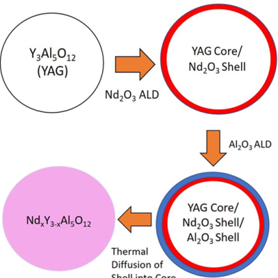
Powder atomic layer deposition process is used to coat nanopowders of host materials (e.g. yttrium aluminum garnet) with optically active neodymium organometal precursor followed by O2/O3 RF plasma to convert to a single layer of Nd2O3. The process can be repeated to build arbitrarily thick layers with custom doping profiles and followed by post-…
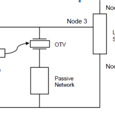
A thyristor will stay conducting until the current through the device is zero (“current zero”) or perhaps slightly negative. LLNL’s approach is to use the opticondistor (“OTV”) to force this current zero in order to force the device into an “off” state. By combining a light-activated thyristor with an OTV, a noise-immune, high efficiency, high-power switching device can be…
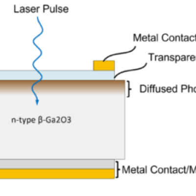
The researchers’ approach leverages the concept that dopants have high diffusivities in Ga2O3; the key lies in the selection of the appropriate dopant. This LLNL invention describes two device types that employ this design:
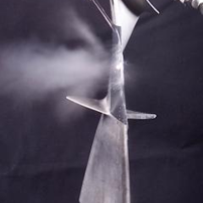
This invention proposes using a pulse laser configured to generate laser pulses and a controller for controlling operation of the pulse laser. The controller is further configured to control the pulse laser to cause the pulse laser to generate at least one of the laser pulses with a spatiotemporally varying laser fluence over a duration of at least one of the laser pulses. The spatiotemporally…
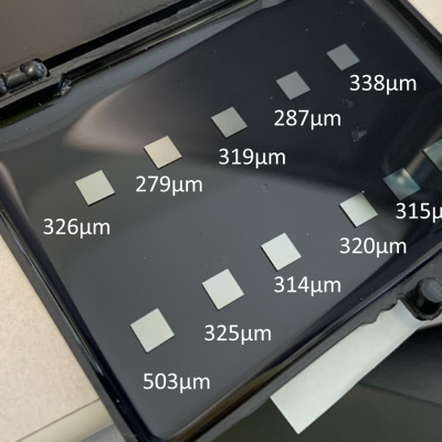
Design and construction of a photoconductive switch requires a diamond photoconductor illuminated by light of a certain excitation wavelength.
Characteristics of the LLNL-developed switch are as follows:
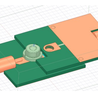
LLNL researchers have invented an ultrafast PCSS to drive a high-power laser diode with arbitrary pulse widths. These devices operate by supplying a high voltage (>10 kV) to one side of the switch. A short pulse of light illuminates the semiconductor, instantly turning it from highly resistive to highly conductive. Ultrawide bandgap (UWBG) semiconductors are used to achieve sub-…

A set of images generated by multiple passes over the same area can be coherently integrated by this technology developed by LLNL researchers. The primary difficulty with coherently combining different passes is registering the images obtained from each pass, particularly if a pass only partially covers a given area.
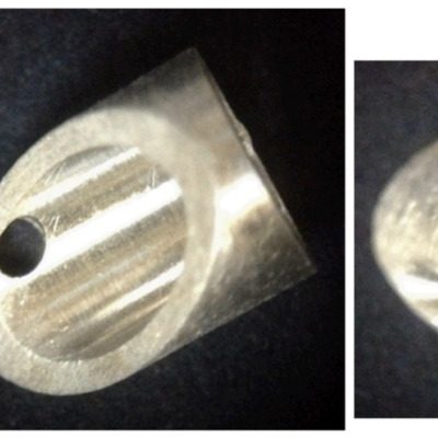
U.S. Patent No. 11,555,965 describes LLNL’s invention of “Illumination Frustums” for photoconductive switches to capture and “frustrate” the light from leaving the frustum. LLNL researcher’s latest novel invention, “Twister Oven”, achieves this by encouraging laser light absorption in a photo conductor material. Light enters the oven twisting and reflecting, making near normal…
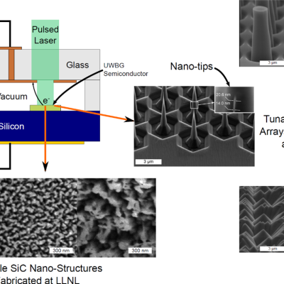
LLNL researchers faced this challenge by bridging the gap between VEDs and solid-state electronics (SSE). Their approach was to create a hybrid vacuum microelectronic device (VMD) architecture that combines the properties of vacuum as the electronic medium and the compact form factor and manufacturing scalability of semiconductor microelectronic chips.
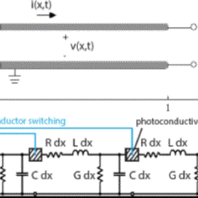
Design and construction of a photoconductive switch requires a diamond photoconductor illuminated by light of a certain excitation wavelength. The diamond material is specifically doped with substitutional nitrogen, which act as a source of electrons. The device architecture allows maximum light entering the aperture. The top and bottom electrodes are made of ultra wide band…
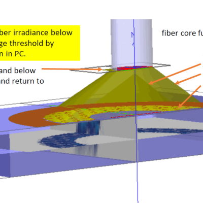
The approach is to use a custom-designed frustrum and attach it to the optical fiber that connects to the PCSS. Light from the fiber enters the frustrum, spreads out, and enters the PCSS. Any unabsorbed light re-enters the frustrum and, because of its geometry, reflects back into the PCSS itself with only a negligible fraction escaping from the fiber. The shape of the novel…
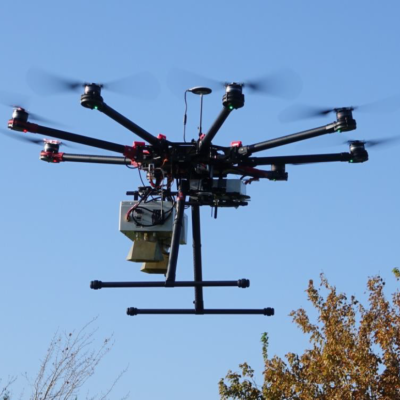
LLNL researchers have developed a lightweight drone-based GPR array that when flown over a surface with laid and/or buried objects could image the field of view and be able to detect targets and discriminate them from clutter. The imaging method employs a modified multi-static architecture to provide the highest signal to noise with the lowest system weight, making it ideal for airborne or…
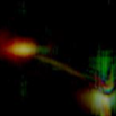
This technology uses three different frequency bands to create intensity maps of returned signals. Signals have traditionally been displayed as raw return data. The intensity of the return is represented by level of brightness. Assignment of a scalar value for intensity is used to determine the brightness of the image. In this technology, each frequency is given a designated…

LLNL has developed a wide band (WB) ground penetrating radar (GPR) technology to detect and image buried objects under a moving vehicle. Efficient and high performance processing algorithms reconstruct images of buried or hidden objects in two or three dimensions under a scanning array. The technology includes a mobile high-performance computing system allowing GPR array sensor data to be…
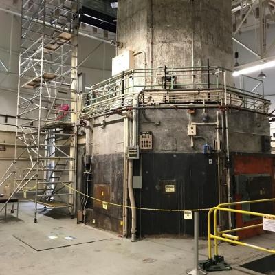
The new LLNL technique works by transiently removing and trapping concrete or rock surface material, so that contaminants are confined in a manner that is easy to isolate and remove. Our studies suggest that 10 m2 of surface could be processed per hour. The technique easily scales to more surface/hr.


