
LLNL researchers have designed and developed a novel high-density, high-channel count 3D connector that enables hundreds or thousands of nonpermanent connections within a compact footprint. The connector addresses limitations of currently used conventional approaches that were described previously, which have an artificial ceiling on the number of recording sites of modern devices of no more…
Image

This invention proposes to engineer the current density along the length of a laser diode to overcome the penalty associated with non-uniformity resulting from asymmetry in the gain, photon or carrier density despite having uniform contact. Optimizing the current density profile enables diode lasers to operate with greater power conversion efficiency or operate with equivalent power conversion…
Image

This invention proposes to engineer the temperature dependence of the emission wavelength of LEDs and laser diodes. The approach is to use a strain-inducing coating to counteract the intrinsic temperature coefficient of the emission wavelength of the LED or laser diode device thereby rendering it athermal. This invention avoids additional complexity, size, weight and power dissipation of…
Image

This invention proposes a method to overcome the key limitation of electrically pumped lasers based on AlN, AlGaN, or AlInGaN, namely the lack of suitable shallow donor and acceptor dopants. As the band gap of these materials increases (and the emission wavelength decreases), both electrons and holes require greater thermal energies in order to ionize.
Image
Laser diode lensing effect can be substantially reduced by creating a pattern interface such that the substrate is only attached at the diode mesa. This is achieved by either creating a pattern solder joint and/or pattern substrate.
Image
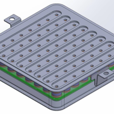
Many of the disadvantages of current interface devices can be overcome with LLNL’s novel interface design, which relies on area array distribution where independent interface connector subassemblies are positioned in a planar grid. Not only is the interface device expandable area-wise (without increasing contact force), but it could also be expanded height-wise, with multiple layers of these…
Image
Commercial fiber optic cables are the current standard for carrying optical signals in industries like communications or medical devices. However, the fibers are made of glass, which do not have favorable characteristics for applications that require flexibility and re-routing, e.g. typically brittle, limited selection of materials, dimension constraints.
Image
LLNL has developed a brain-on-a-chip system with a removable cell-seeding funnel to simultaneously localize neurons from various brain regions in an anatomically relevant manner and over specific electrode regions of a MEA. LLNL’s novel, removable cell seeding funnel uses a combination of 3D printing and microfabrication that allows neurons from select brain regions to easily be seeded into…