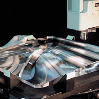
This invention takes advantage of the high water-solubility of key NIF KDP crystal optics and uses water as an etchant to remove surface defects and improve the laser induced damage threshold. Since pure water etches KDP too fast, this invention is to disperse water as nanosized droplets in a water-in-oil micro-emulsion. While in a stable micro-emulsion form, the surfactant additives prevent…
Image
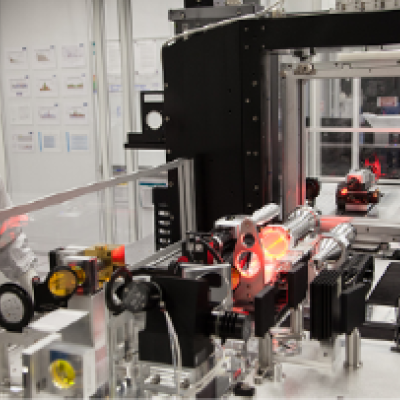
This invention proposes to use laser induced melting/softening to locally reshape the form of a glass optic. The local glass densification that results induces predictable stresses that through plate deformation mechanics yield a deterministic methodology for arbitrarily reshaping an optic surface figure and wavefront without the need to remove material.
Image

The approach is to leverage the fact that a momentary “load” equal to the power transmission line impedance, (Z0), during the transient can suppress its propagation. Z(0) is typically a fixed impedance of several hundred ohms based on the geometry of most single wire transmission lines.
So, an isolated self-powered opticondistor (OTV) system may provide an ultrafast method of…
Image

LLNL’s novel approach is to use diamond substrates with the desired donor (nitrogen) and acceptor (boron) impurities. In order to optically activate these deep impurities, the invention requires at least one externally or internally integrated light source. The initial exposure to light can set up the desired conduction current, after which the light source could be turned off. Even with…
Image

Instead of producing individual DSRDs and bonding them, Tunnel DSRD's entire stack structure is grown epitaxially on a n- or p-type silicon wafer, resulting in a novel, “monolithic” stacked DSRD. A tunnel diode is essentially a diode with very highly doped p and n regions such that the reverse breakdown voltage is 200 meV or lower.
Image
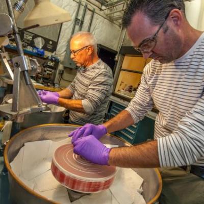
LLNL's Slurry Stabilization Method provides a chemical means of stabilizing a polishing compound in suspension at working concentrations without reducing the rate of material removal. The treated product remains stable for many months in storage.