Image
Fabrication of height modulated and tapered features in fused silica

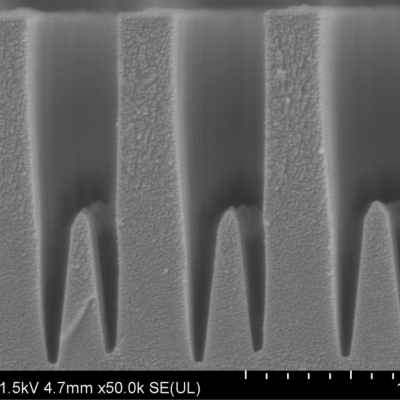
This LLNL invention allows for the fabrication of complex waveplate features and topologies from fused silica, a highly desirable and durable waveplate material.  It also is a unique technique for density multiplication and high-fidelity bidirectional deposition, which can create optical components that are generally for entirely new classes of optical materials.

Left Image Caption…

Image
Standing in LLNL’s Center for Micro Nano Technology, Nathan Ray holds a marvel of optical engineering, a 5-centimeter metasurface optic

This LLNL invention concerns a method for patterning the index of refraction by fabricating a spatially invariant metasurface, and then apply spatially varied mechanical loading to compress the metasurface features vertically and spread them radially. In doing so, the index of refraction can be re-written on the metasurface, thus enabling index patterning. This process allows rapid 'rewriting…

Image
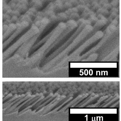
SEM image of etched metasurface with angled features

This novel invention specifically enables the fabrication of arbitrarily tailored birefringence characteristics in nano-structured meta-surfaces on non-birefringent substrates (e.g. fused silica). The birefringent nano-structured meta-surface is produced by angled directional reactive ion beam etching through a nano-particle mask. This method enables the simultaneous tailoring of refractive…

Image
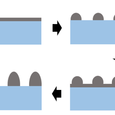
Schematic of one methodology for achieving a thicker substrate engraved meta-surface (SEMS) layer

This invention (US Patent No. 11,294,103) is an extension of another LLNL invention, US Patent No. 10,612,145, which utilizes a thin sacrificial metal mask layer deposited on a dielectric substrate (e.g. fused silica) and subsequently nanostructured through a laser generated selective thermal de-wetting process.

Image
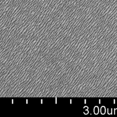
Scanning electron micrograph of scalable, grating-like nanoscale metal mask (line period ~35 nm)

This invention consists of a method of forming nanoscale metal lines to produce a grating-like mask with wide area coverage over the surface of a durable optical material such as fused silica. Subsequent etching processes transfer the metal mask to the underlying substrate forming a birefringent metasurface. This method enables the production of ultrathin waveplates for high power laser…

Image
Scanning electron micrograph of bulk metamaterial structures fabricated at LLNL

Heat sensitive materials such as piezoelectric and MEMS devices and assemblies, magnetic sensors, nonlinear optical crystals, laser glass or solid-state laser materials, etc. cannot be exposed to excess temperatures which in the context of this invention, means materials that cannot be exposed to temperatures greater than 50°C (122°F). LLNL’s invention describes a low-temperature method of…

Image
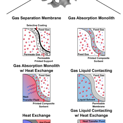
Potential reactor configurations with printed TPMS scaffolds

LLNL researchers have devised a set of design principles that facilitates the development of practical TPMS-based two fluid flow reactors.; included in the design are these new concepts:

Image
Filled (8,8) (left) and (15,15) (right) CNTs with [EMIM+][BF4- ] using SGTI with the proposed spliced soft-core potential (SSCP) approach

LLNL researchers have developed a novel simulation methodology using slow growth thermodynamic integration (SGTI) utilizing spliced soft-core interaction potential (SSCP).  The approach to filling the molecular enclosures is a nonphysical one.  Rather than filling the pores from the open ends this method creates steps in the algorithm that allow molecules to pass through the pore…

Image
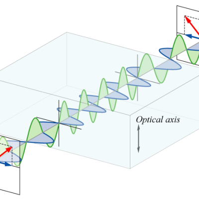
Linearly polarized light entering a half-wave plate can be resolved into two waves, parallel and perpendicular to the optic axis of the waveplate ("Waveplate" by Bob Mellish is licensed under CC BY-SA 3.0).

This novel method of producing waveplates from isotropic optical materials (e.g. fused silica) consists of forming a void-dash metasurface using the following process steps:

Image
Nanoporus gold

By combining 3D printing and dealloying., researchers at LLNL have developed a method for fabricating metal foams with engineered hierarchical architectures consisting of pores at least 3 distinct length scales. LLNL’s method uses direct ink writing (DIW), a 3D printing technique for additive manufacturing to fabricate hierarchical nanoporous metal foams with deterministically controlled 3D…

Image
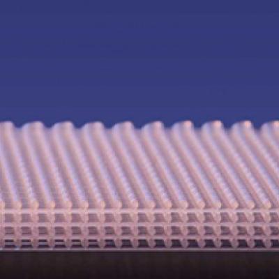
energy_absorbing_material

To overcome limitations with cellular silicone foams, LLNL innovators have developed a new 3D energy absorbing material with tailored/engineered bulk-scale properties. The energy absorbing material has 3D patterned architectures specially designed for specific energy absorbing properties. The combination of LLNL's capabilities in advanced modeling and simulation and the additive…