
For this method, a Silicon on Insulator (SOI) wafer is used to tailor etch rates and thickness in initial steps of the process. The simple three step process approach is comprised of grayscale lithography, deep reactive-ion etch (DRIE) and liftoff of the SOI wafer. The liftoff process is used to dissolve the insulating layer, thus separating sections of the wafer as individual silicon…
Image
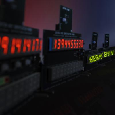
LLNL's method of equivalent time sampling incorporates an embedded system that generates the pulses used to trigger the external circuit and the data acquisition (DAQ). This removes the external reference clock, allowing the overall system clock rate to change based on the ability of the embedded system. The time delays needed to create the time stepping for equivalent time sampling is done by…
Image

LLNL’s Optically-based Interstory Drift Meter System provides a means to accurately measure the dynamic interstory drift of a vibrating building (or other structure) during earthquake shaking. This technology addresses many of the shortcomings associated with traditional strong motion accelerometer based building monitoring.
LLNL’s discrete diode position sensitive device is a newly…
Image

The invention relates to a measurement method and system for capturing both the amplitude and phase temporal profile of a transient waveform or a selected number of consecutive waveforms having bandwidths of up to about 10 THz in a single shot or in a high repetition rate mode. The invention consists of an optical preprocessor which can then output a time-scaled replica of the input signal to…