

For this method, a Silicon on Insulator (SOI) wafer is used to tailor etch rates and thickness in initial steps of the process. The simple three step process approach is comprised of grayscale lithography, deep reactive-ion etch (DRIE) and liftoff of the SOI wafer. The liftoff process is used to dissolve the insulating layer, thus separating sections of the wafer as individual…
Image
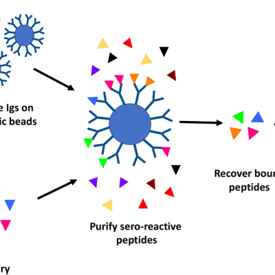
High throughput discovery of linear B-cell epitopes for the development of vaccines and therapeutics
LLNL’s high throughput method involves proteome-wide screening for linear B-cell epitopes using native proteomes isolated from a pathogen of interest and convalescent sera from immunized animals.
Image
LLNL has developed a novel process of production, isolation, characterization, and functional re-constitution of membrane-associated proteins in a single step. In addition, LLNL has developed a colorimetric assay that indicates production, correct folding, and incorporation of bR into soluble nanolipoprotein particles (NLPs).
LLNL has developed an approach, for formation of NLP/…