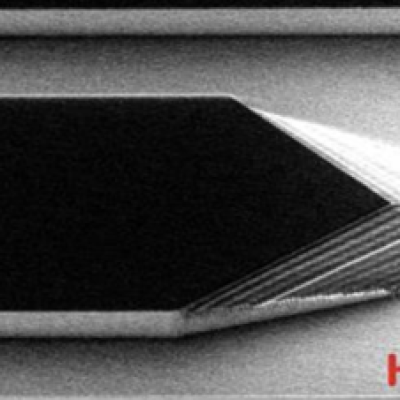
LLNL researchers have developed an approach to form silicon carbide (and diamond) nanoneedles using plasma etching that create micro pillars followed by chemical etching of the pillars in forming gas containing hydrogen and nitrogen. Combining these two etching processes allow for fabrication of micro- and nanoneedles that are thinner and sharper than conventionally fabricated needles.
Keywords
- Show all (53)
- Imaging Systems (9)
- Photoconductive Semiconductor Switches (PCSS) (9)
- Semiconductors (7)
- Optical Switches (5)
- Power Electronics (4)
- Additive Manufacturing (2)
- Computing (2)
- Electric Grid (2)
- Sensors (2)
- Spectrometers (2)
- 3D Electronics (1)
- Analysis (1)
- Brain Computer Interface (BCI) (1)
- Compact Space Telescopes (1)
- Optical Sensors (1)
- Particle Accelerators (1)
- Quantum Science (1)
- (-) Instrumentation (1)
- (-) MEMS Sensors (1)
Image

For this method, a Silicon on Insulator (SOI) wafer is used to tailor etch rates and thickness in initial steps of the process. The simple three step process approach is comprised of grayscale lithography, deep reactive-ion etch (DRIE) and liftoff of the SOI wafer. The liftoff process is used to dissolve the insulating layer, thus separating sections of the wafer as individual…


