
LLNL researchers have developed a method to of crosslinking, polymerizing or otherwise covalently coupling a subset of nitroaromatic and nitramine explosive molecules and compositions. Energetic materials manufactured using the novel method can be used ‘neat’ or as an energetic binder phase for another unmodified energetic compound. The approach may also be employed to co-…
Image

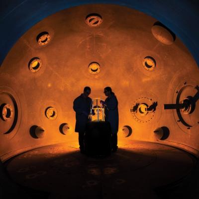
LLNL developed a novel SOS diode structure starting with a n-type silicon wafer. On the appropriate sides of the wafer, donor and acceptor dopants with specifically designed and optimized concentration profiles are diffused in the structure. Crucially, an extra n-region is introduced to the structure to address pre-pulses. The result is a SOS diode with an optimized p+/p/n-…
Image
LLNL has developed a method that adds a polyamine based crosslinker and an acid receptor, based on MgO nanoparticles into a polymer bonded PBX, where the polymer binder is a fluoropolymer containing vinylidene difluoride functionality. Crosslinking kinetics can then be controlled by selecting an appropriate amine structure, pressing temperature and optionally the addition of a chemical…
Image
LLNL researchers uses Additive Manufacturing (AM) to create reinforcing scaffolds that can be integrated with High Explosives (HE) or solid rocket fuel with minimal volume fraction. Its main benefit is to create stability in harsh field conditions. Its secondary benefit is providing another method to finely tune blast performance or fuel burn. Creating complex shapes with structural…
Image

The approach is to leverage the fact that a momentary “load” equal to the power transmission line impedance, (Z0), during the transient can suppress its propagation. Z(0) is typically a fixed impedance of several hundred ohms based on the geometry of most single wire transmission lines.
So, an isolated self-powered opticondistor (OTV) system may provide an ultrafast method of…
Image

LLNL’s novel approach is to use diamond substrates with the desired donor (nitrogen) and acceptor (boron) impurities. In order to optically activate these deep impurities, the invention requires at least one externally or internally integrated light source. The initial exposure to light can set up the desired conduction current, after which the light source could be turned…
Image

Instead of producing individual DSRDs and bonding them, Tunnel DSRD's entire stack structure is grown epitaxially on a n- or p-type silicon wafer, resulting in a novel, “monolithic” stacked DSRD. A tunnel diode is essentially a diode with very highly doped p and n regions such that the reverse breakdown voltage is 200 meV or lower.