
This portfolio was organized to group innovations that might not be categorized in the other portfolios. Instruments are full systems integrated to perform complex electrical or mechanical work. Sensors are devices that detect, measure, or locate a physical property. Electronics are devices that manipulate electrons or control electrical energy, and the manufacturing processes that fabricate them.
Portfolio News and Multimedia
The trade journal R&D World Magazine recently announced the winners of the awards, often called the “Oscars of innovation,” recognizing new commercial products, technologies and materials that are available for sale or license for their technological significance.
Lawrence Livermore National Laboratory (LLNL) scientists and engineers have earned four awards among the top 100 inventions worldwide. With this year’s results, the Laboratory has now collected a total of 186 R&D 100 awards since 1978.
Submitted through LLNL’s Innovation and Partnerships Office (IPO), these awards recognize the impact that Livermore innovation, in collaboration with industry partners, can have on the U.S. economy as well as globally.
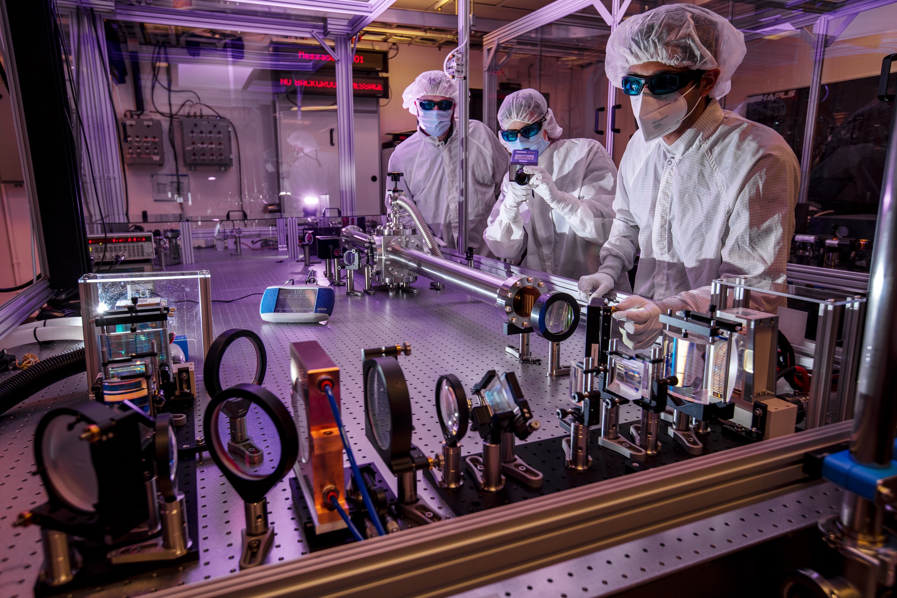
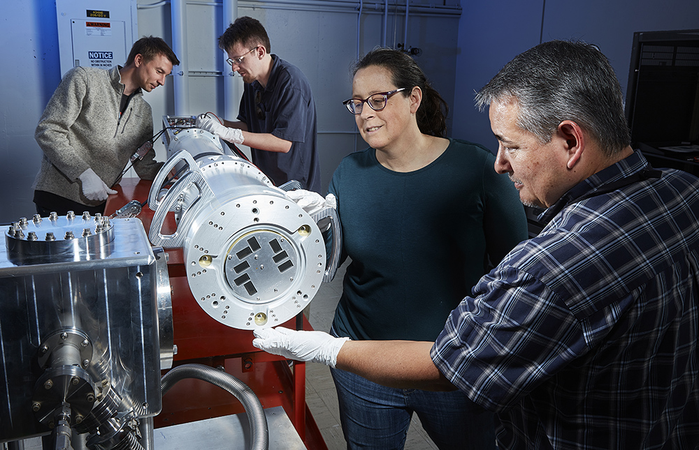
Decades of cutting-edge laser, optics and plasma physics research at Lawrence Livermore National Laboratory (LLNL) played a key role in the underlying science that the semiconductor industry uses to manufacture advanced microprocessors. Now a new research partnership led by LLNL aims to lay the groundwork for the next evolution of extreme ultraviolet (EUV) lithography, centered around a Lab-developed driver system dubbed the Big Aperture Thulium (BAT) laser.
LLNL plasma physicists, Brendan Reagan and Jackson Williams, are the project’s co-lead principal investigators. The project includes scientists from SLAC National Accelerator Laboratory; ASML San Diego; and the Advanced Research Center for Nanolithography (ARCNL), a public-private research center based in the Netherlands.
Funded through DOE’s Unlocking Lasting Transformative Resiliency Advances by Faster Actuation of power Semiconductor Technologies (ULTRAFAST) program, LLNL researchers (in Engineering) will develop an optically-controlled semiconductor transistor to enable future grid control systems to accommodate higher voltage and current than state-of-the-art devices. (Award amount: $3,000,000) while LLNL licensee Opcondys will develop a light-controlled grid protection device to suppress destructive, sudden transient surges on the grid such as those caused by lightning and electromagnetic pulses. (Award amount: $3,178,977)

LLNL developed a novel SOS diode structure starting with a n-type silicon wafer. On the appropriate sides of the wafer, donor and acceptor dopants with specifically designed and optimized concentration profiles are diffused in the structure. Crucially, an extra n-region is introduced to the structure to address pre-pulses. The result is a SOS diode with an optimized p+/p/n-…

The approach is to use appropriately doped semi-insulating gallium nitride to provide a high damage tolerant photoconductor with high responsivity to various pump wavelength light. Mn, C, or Fe are used as dopants to provide a source of electrons or holes that can be excited. This is combined with the use of dichroic antireflection coating at the GaN/polyimide/liquid crystal…

LLNL researchers has developed designs to augment WBG/UWBG-based OALVs to improve their power handling capability under CW operational environments. These designs include:

The approach is to leverage the fact that a momentary “load” equal to the power transmission line impedance, (Z0), during the transient can suppress its propagation. Z(0) is typically a fixed impedance of several hundred ohms based on the geometry of most single wire transmission lines.
So, an isolated self-powered opticondistor (OTV) system may provide an ultrafast method of…

LLNL’s novel approach is to use diamond substrates with the desired donor (nitrogen) and acceptor (boron) impurities. In order to optically activate these deep impurities, the invention requires at least one externally or internally integrated light source. The initial exposure to light can set up the desired conduction current, after which the light source could be turned…

Instead of producing individual DSRDs and bonding them, Tunnel DSRD's entire stack structure is grown epitaxially on a n- or p-type silicon wafer, resulting in a novel, “monolithic” stacked DSRD. A tunnel diode is essentially a diode with very highly doped p and n regions such that the reverse breakdown voltage is 200 meV or lower.

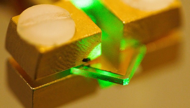
Design and construction of a photoconductive switch requires a diamond photoconductor illuminated by light of a certain excitation wavelength. The diamond material is specifically doped with substitutional nitrogen, which act as a source of electrons. The device architecture allows maximum light entering the aperture. The top and bottom electrodes are made of ultra wide band…

The approach is to use a custom-designed frustrum and attach it to the optical fiber that connects to the PCSS. Light from the fiber enters the frustrum, spreads out, and enters the PCSS. Any unabsorbed light re-enters the frustrum and, because of its geometry, reflects back into the PCSS itself with only a negligible fraction escaping from the fiber. The shape of the novel…

LLNL researchers have designed and tested performance characteristics for a multichannel pyrometer that works in the NIR from 1200 to 2000 nm. A single datapoint without averaging can be acquired in 14 microseconds (sampling rate of 70,000/s). In conjunction with a diamond anvil cell, the system still works down to about 830K.

The Optical Transconductance Varistor (OTV, formerly Opticondistor) overcomes depletion region voltage limitations by optically exciting wide bandgap materials in a compact package. A 100μm thick crystal could have the capability approaching 40kV and would replace numerous equivalent junction devices. Thus, unlike present junction transistors or diodes, this wide bandgap device can be stacked…