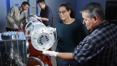
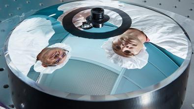
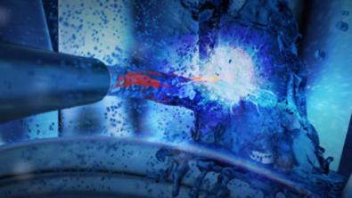
The Lawrence Livermore National Laboratory is home to the world’s largest laser system, the National Ignition Facility (NIF). The NIF with its 192 beam lines and over 40,000 optics has been an engine of innovation for lasers and optics technologies for the last couple of decades. The Lasers and Optics intellectual property portfolio is the culmination of the many groundbreaking developments in high energy, high peak power and ultrashort pulse laser system design and operation, including technologies related to Laser Diodes, Fiber & Disk Lasers, Compact Telescopes, High Damage Threshold Gratings, High Power Optical Components and their Fabrication and Coating Techniques. The thrust of the research and development at the NIF has been to realize novel approaches for laser systems, optical components and their applications that are more compact and higher efficiency while reliably delivering ever higher energy and peak power capabilities required in the furtherance of LLNL’s missions in Stockpile Stewardship and High Energy Density Science.

Portfolio News and Multimedia

Image
The power of partnerships: How LLNL laser technology is transforming industrial manufacturing

It’s the late 1990s. Lloyd Hackel and Brent Dane are researchers in Lawrence Livermore National Laboratory’s (LLNL) laser science and technology program.

They’re developing laser technology for X-ray lithography and satellite imaging research for the Department of Defense when the phone rings. On the line is Curtiss-Wright’s Metal Improvement Company (MIC) asking about something Hackel and Dane haven’t worked on before: high-peak-power laser peening for commercial applications in manufacturing.

This is an example of how LLNL’s mission-focused work advancing national security can lead to technology spin-offs with commercial importance through the Innovation and Partnerships Office (IPO).

For more, watch the YouTube video.

Image
LLNL selected to lead next-gen extreme ultraviolet lithography research

Decades of cutting-edge laser, optics and plasma physics research at Lawrence Livermore National Laboratory (LLNL) played a key role in the underlying science that the semiconductor industry uses to manufacture advanced microprocessors. Now a new research partnership led by LLNL aims to lay the groundwork for the next evolution of extreme ultraviolet (EUV) lithography, centered around a Lab-developed driver system dubbed the Big Aperture Thulium (BAT) laser.

LLNL plasma physicists, Brendan Reagan and Jackson Williams, are the project’s co-lead principal investigators. The project includes scientists from SLAC National Accelerator Laboratory; ASML San Diego; and the Advanced Research Center for Nanolithography (ARCNL), a public-private research center based in the Netherlands.

Image
LLNL and Starris: Optimax Space Systems announce partnership for monolithic telescope technology

Starris: Optimax Space Systems and Lawrence Livermore National Laboratory (LLNL) have entered a commercialization partnership for LLNL’s patented monolithic telescope technology, which accelerates rapid deployment of modular optical designs for high-resolution or high-sensitivity space imagery.

Starris has collaborated over the last decade with LLNL’s Space Program to develop the monolithic telescope technology and will manufacture — at scale and with customization options — the precision-fabricated optical lens that forms the image in the telescope. The collaboration with LLNL is now extended via a government-use license for commercializing the technology through LLNL’s Innovation and Partnerships Office (IPO).

Lasers and Optics Technologies

Image
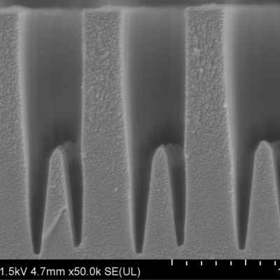
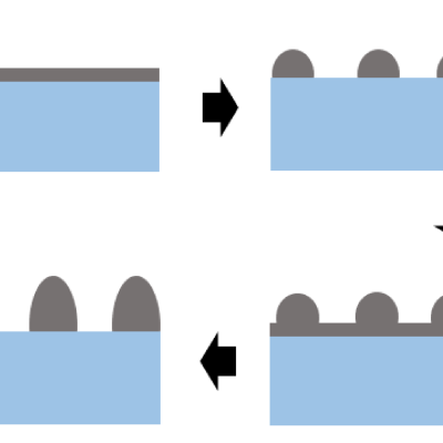
Fabrication of height modulated and tapered features in fused silica

This LLNL invention allows for the fabrication of complex waveplate features and topologies from fused silica, a highly desirable and durable waveplate material.  It also is a unique technique for density multiplication and high-fidelity bidirectional deposition, which can create optical components that are generally for entirely new classes of optical materials.

Left Image Caption…

Image
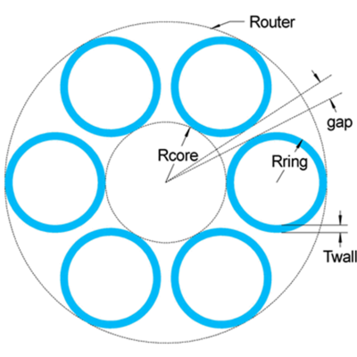
Schematic of six-ring design for IL-13352

This LLNL invention proposes a new microstructured large mode area fiber design that enhances the confinement of the core mode while strongly suppressing thermal or scattering mediated dynamic couplings with higher order modes thought to be responsible for generating undesirable Transverse Mode Instabilities. The design accomplishes higher order mode suppression and core mode confinement by…

Image
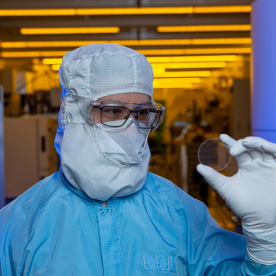
Standing in LLNL’s Center for Micro Nano Technology, Nathan Ray holds a marvel of optical engineering, a 5-centimeter metasurface optic

This LLNL invention concerns a method for patterning the index of refraction by fabricating a spatially invariant metasurface, and then apply spatially varied mechanical loading to compress the metasurface features vertically and spread them radially. In doing so, the index of refraction can be re-written on the metasurface, thus enabling index patterning. This process allows rapid 'rewriting…

Image
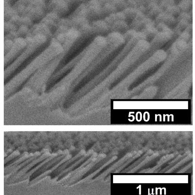
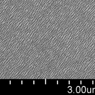
SEM image of etched metasurface with angled features

This novel invention specifically enables the fabrication of arbitrarily tailored birefringence characteristics in nano-structured meta-surfaces on non-birefringent substrates (e.g. fused silica). The birefringent nano-structured meta-surface is produced by angled directional reactive ion beam etching through a nano-particle mask. This method enables the simultaneous tailoring of refractive…

Image
Schematic of one methodology for achieving a thicker substrate engraved meta-surface (SEMS) layer

This invention (US Patent No. 11,294,103) is an extension of another LLNL invention, US Patent No. 10,612,145, which utilizes a thin sacrificial metal mask layer deposited on a dielectric substrate (e.g. fused silica) and subsequently nanostructured through a laser generated selective thermal de-wetting process.

Image
Scanning electron micrograph of scalable, grating-like nanoscale metal mask (line period ~35 nm)

This invention consists of a method of forming nanoscale metal lines to produce a grating-like mask with wide area coverage over the surface of a durable optical material such as fused silica. Subsequent etching processes transfer the metal mask to the underlying substrate forming a birefringent metasurface. This method enables the production of ultrathin waveplates for high power laser…

Image
Scanning electron micrograph of bulk metamaterial structures fabricated at LLNL

Heat sensitive materials such as piezoelectric and MEMS devices and assemblies, magnetic sensors, nonlinear optical crystals, laser glass or solid-state laser materials, etc. cannot be exposed to excess temperatures which in the context of this invention, means materials that cannot be exposed to temperatures greater than 50°C (122°F). LLNL’s invention describes a low-temperature method of…

Image
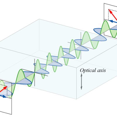
Linearly polarized light entering a half-wave plate can be resolved into two waves, parallel and perpendicular to the optic axis of the waveplate ("Waveplate" by Bob Mellish is licensed under CC BY-SA 3.0).

This novel method of producing waveplates from isotropic optical materials (e.g. fused silica) consists of forming a void-dash metasurface using the following process steps:

Image
grating_optic2

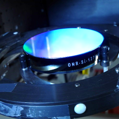
Livermore Lab's SBC grating optics benefit from the combination of the following key technologies:

  • LLNL proprietary optical coating designs utilizing >100 thin film layers – enables ultra-low-loss, ppm transmission levels through the coating, high diffraction efficiency, and large bandwidth.
  • LLNL proprietary dispersive surface relief structure…