

The approach is to use appropriately doped semi-insulating gallium nitride to provide a high damage tolerant photoconductor with high responsivity to various pump wavelength light. Mn, C, or Fe are used as dopants to provide a source of electrons or holes that can be excited. This is combined with the use of dichroic antireflection coating at the GaN/polyimide/liquid crystal…
Image
This LLNL invention allows for the fabrication of complex waveplate features and topologies from fused silica, a highly desirable and durable waveplate material. It also is a unique technique for density multiplication and high-fidelity bidirectional deposition, which can create optical components that are generally for entirely new classes of optical materials.
Left Image Caption…
Image
LLNL researchers have continued to develop their pioneering DIW 3D-printed glass optics technology that allows for the 3D printing of single- and multi-material optical glass compositions in complex shapes. This LLNL invention further proposes incorporating dopants (including, but not limited to TiO2 and Pd) into slurries and inks for 3D printing of glass components that can then be directly…
Image
This LLNL invention concerns a method for patterning the index of refraction by fabricating a spatially invariant metasurface, and then apply spatially varied mechanical loading to compress the metasurface features vertically and spread them radially. In doing so, the index of refraction can be re-written on the metasurface, thus enabling index patterning. This process allows rapid 'rewriting…
Image
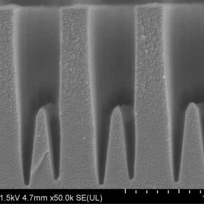
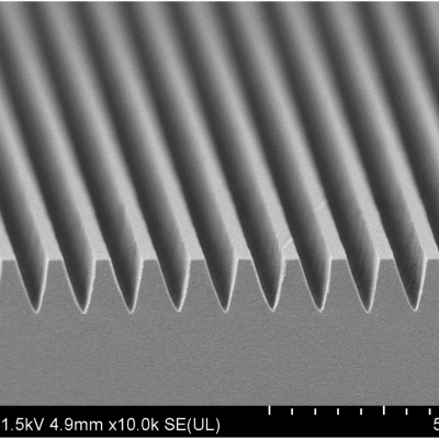
This novel invention specifically enables the fabrication of arbitrarily tailored birefringence characteristics in nano-structured meta-surfaces on non-birefringent substrates (e.g. fused silica). The birefringent nano-structured meta-surface is produced by angled directional reactive ion beam etching through a nano-particle mask. This method enables the simultaneous tailoring of refractive…
Image
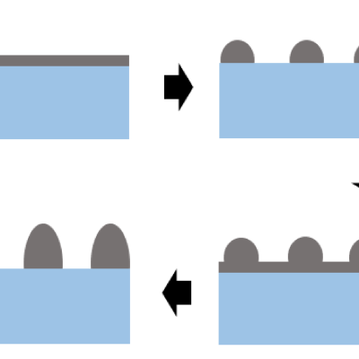
This invention (US Patent No. 11,294,103) is an extension of another LLNL invention, US Patent No. 10,612,145, which utilizes a thin sacrificial metal mask layer deposited on a dielectric substrate (e.g. fused silica) and subsequently nanostructured through a laser generated selective thermal de-wetting process.
Image
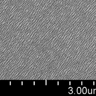
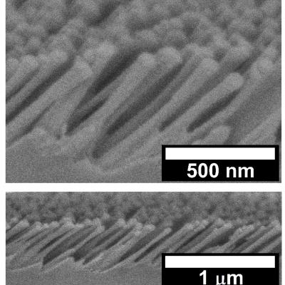
This invention consists of a method of forming nanoscale metal lines to produce a grating-like mask with wide area coverage over the surface of a durable optical material such as fused silica. Subsequent etching processes transfer the metal mask to the underlying substrate forming a birefringent metasurface. This method enables the production of ultrathin waveplates for high power laser…
Image
Heat sensitive materials such as piezoelectric and MEMS devices and assemblies, magnetic sensors, nonlinear optical crystals, laser glass or solid-state laser materials, etc. cannot be exposed to excess temperatures which in the context of this invention, means materials that cannot be exposed to temperatures greater than 50°C (122°F). LLNL’s invention describes a low-temperature method of…
Image
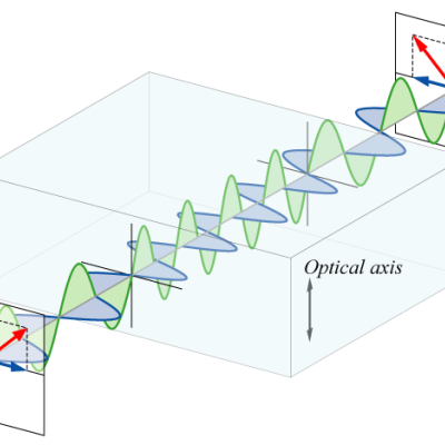
This novel method of producing waveplates from isotropic optical materials (e.g. fused silica) consists of forming a void-dash metasurface using the following process steps: