
LLNL researchers has developed a composite copper current collector formulation readily used in DIW 3D printing to guide lithium-ion plating/dissolution during charging and discharging cycles.
Image

LLNL researchers have developed an approach to form silicon carbide (and diamond) nanoneedles using plasma etching that create micro pillars followed by chemical etching of the pillars in forming gas containing hydrogen and nitrogen. Combining these two etching processes allow for fabrication of micro- and nanoneedles that are thinner and sharper than conventionally fabricated needles.
Image

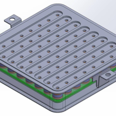
LLNL researchers have designed and developed a novel high-density, high-channel count 3D connector that enables hundreds or thousands of nonpermanent connections within a compact footprint. The connector addresses limitations of currently used conventional approaches that were described previously, which have an artificial ceiling on the number of recording sites of modern devices of no more…
Image

LLNL’s invention is a photopolymerizable polymer resin that consists of one or more nitrile-functional based polymers. The resin is formulated for SLA based 3D printing allowing for the production of nitrile-containing polymer components that can then be thermally processed into a conductive, highly graphitic materials. The novelty of the invention lies in (1) the photo-curable nitrile-…
Image

This invention works by imaging an ultrafast pulse diffracted from a large grating onto a spatial light modulator (SLM) thereby directly transcribing an arbitrary record on a pulse front tilted (PFT) ultrafast pulse. The grating generates PFT of the input pulse, and the SLM provides temporal control of the pulse through the space-to-time mapping of the tilted pulse. Coupling this patterned…
Image
LLNL researchers have developed a fabrication process for creating 3D random interdigitated architectures of anodes and cathodes, eliminating the need for a membrane to separate them. This approach is similar to the repeating interdigitated multi-electrode architectures that also were developed at LLNL.
Image
This invention exploits the non-linearities of optical Mach-Zehnder (MZ) electrooptic modulators to enhance small signal dynamic range at higher bandwidths. A linear photodiode (PD) converts the amplified optical signal output from the MZ back to an electrical signal completing an Electrical-Optical-Electrical (EOE) conversion cycle. The dynamic range can be further enhanced by daisy chaining…
Image
LLNL researchers have developed novel advanced manufactured biomimetic 3D-TPMS (triply periodic minimal surface) membrane architectures such as a 3D gyroid membrane. The membrane is printed using LLNL's nano-porous photoresist technology. LLNL’s 3D-TPMS membranes consist of two independent but interpenetrating macropore flow channel systems that are separated by a thin nano-porous wall…
Image

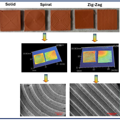
Improving the active material of the Zn anode is critical to improving the practicality of Zn-MnO2 battery technology. LLNL researchers have developed a new category of 3D structured Zn anode using a direct-ink writing (DIW) printing process to create innovative hierarchical architectures. The DIW ink, which is a gel-based mixture composed of zinc metal powder and organic binders, is…
Image
To get the best of both worlds – the sensitivity of LC-MS with the speed of PS-MS – and a functional substrate that can maintain sample integrity, LLNL researchers looked to 3D printing. They have patented a novel approach to create lattice spray substrates for direct ionization mass spectroscopy using 3D-printing processes.
Image

LLNL researchers, through careful control over the chemistry, network formation, and crosslink density of the ink formulations as well as introduction of selected additives, have been successful in preparing 3D printable silicone inks with tunable material properties. For DIW (direct in writing) applications, LLNL has a growing IP portfolio around 3D printable silicone feedstocks for…
Image
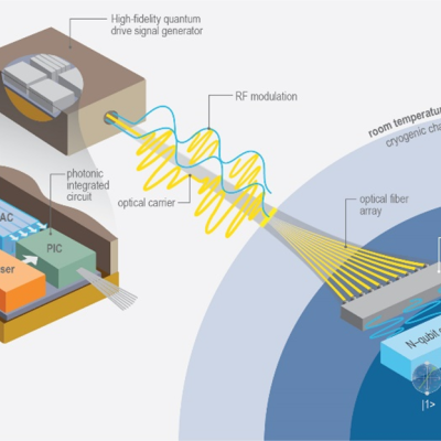
LLNL researchers in the NIF Directorate DoD Technologies RF Photonics Group explored phase modulation solutions to this signal processing challenge. Optical frequency combs offer phase noise characteristics that are orders of magnitude lower than available from commercial microwave references. The Photonics Group researchers recognized that by converting the intensity information into phase,…
Image
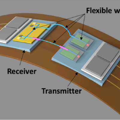
Many of the disadvantages of current interface devices can be overcome with LLNL’s novel interface design, which relies on area array distribution where independent interface connector subassemblies are positioned in a planar grid. Not only is the interface device expandable area-wise (without increasing contact force), but it could also be expanded height-wise, with multiple layers of…
LLNL’s method of 3D printing fiber-reinforced composites has two enabling features:
Image
Commercial fiber optic cables are the current standard for carrying optical signals in industries like communications or medical devices. However, the fibers are made of glass, which do not have favorable characteristics for applications that require flexibility and re-routing, e.g. typically brittle, limited selection of materials, dimension constraints.
Image
LLNL has developed a brain-on-a-chip system with a removable cell-seeding funnel to simultaneously localize neurons from various brain regions in an anatomically relevant manner and over specific electrode regions of a MEA. LLNL’s novel, removable cell seeding funnel uses a combination of 3D printing and microfabrication that allows neurons from select brain regions to easily be seeded into…