
A thyristor will stay conducting until the current through the device is zero (“current zero”) or perhaps slightly negative. LLNL’s approach is to use the opticondistor (“OTV”) to force this current zero in order to force the device into an “off” state. By combining a light-activated thyristor with an OTV, a noise-immune, high efficiency, high-power switching device can be constructed. The…
Image

The approach is to leverage the fact that a momentary “load” equal to the power transmission line impedance, (Z0), during the transient can suppress its propagation. Z(0) is typically a fixed impedance of several hundred ohms based on the geometry of most single wire transmission lines.
So, an isolated self-powered opticondistor (OTV) system may provide an ultrafast method of…
Image

Improving the active material of the Zn anode is critical to improving the practicality of Zn-MnO2 battery technology. LLNL researchers have developed a new category of 3D structured Zn anode using a direct-ink writing (DIW) printing process to create innovative hierarchical architectures. The DIW ink, which is a gel-based mixture composed of zinc metal powder and organic binders, is extruded…
Image
LLNL’s novel approach utilizes a number of techniques to improve reconstruction accuracy:
Image

For this method, a Silicon on Insulator (SOI) wafer is used to tailor etch rates and thickness in initial steps of the process. The simple three step process approach is comprised of grayscale lithography, deep reactive-ion etch (DRIE) and liftoff of the SOI wafer. The liftoff process is used to dissolve the insulating layer, thus separating sections of the wafer as individual silicon…
Image
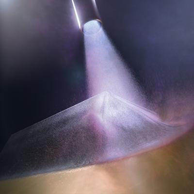
Versatile Cold Spray (VCS) enables deposition of brittle materials, such as thermoelectrics, magnets, and insulators, while retaining their functional properties. Materials can be deposited on substrates or arbitrary shapes with no requirement to match compositions. The VCS system is low cost, easily portable, and easy to use.
VCS has been developed in a collaboration between Lawrence Livermore…
Image
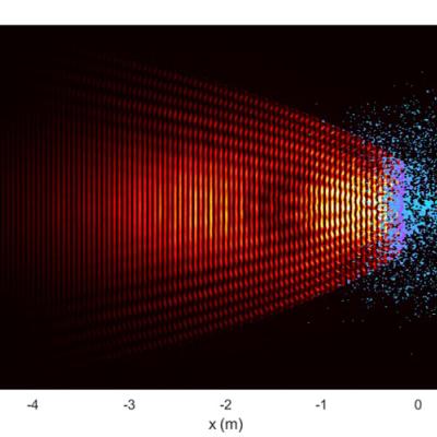
LLNL pioneered the use of tomographic reconstruction to determine the power density of electron beams using profiles of the beam taken at a number of angles. LLNL’s earlier diagnostic consisted of a fixed number of radially oriented sensor slits and required the beam to be circled over them at a fixed known diameter to collect data. The new sensor design incorporates annular slits instead,…
Image

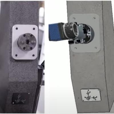
LLNL has developed a compact and low-power cantilever-based sensor array, which has been used to detect various vapor-phase analytes. For further information on the latest developments, see the article "Sniffing the Air with an Electronic Nose."