
LLNL researchers has developed designs to augment WBG/UWBG-based OALVs to improve their power handling capability under CW operational environments. These designs include:
Image
LLNL’s novel approach utilizes a number of techniques to improve reconstruction accuracy:
Image

For this method, a Silicon on Insulator (SOI) wafer is used to tailor etch rates and thickness in initial steps of the process. The simple three step process approach is comprised of grayscale lithography, deep reactive-ion etch (DRIE) and liftoff of the SOI wafer. The liftoff process is used to dissolve the insulating layer, thus separating sections of the wafer as individual silicon…
Image

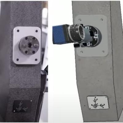
Design and construction of a photoconductive switch requires a diamond photoconductor illuminated by light of a certain excitation wavelength. The diamond material is specifically doped with substitutional nitrogen, which act as a source of electrons. The device architecture allows maximum light entering the aperture. The top and bottom electrodes are made of ultra wide band gap (UWBG)…
Image

The approach is to use a custom-designed frustrum and attach it to the optical fiber that connects to the PCSS. Light from the fiber enters the frustrum, spreads out, and enters the PCSS. Any unabsorbed light re-enters the frustrum and, because of its geometry, reflects back into the PCSS itself with only a negligible fraction escaping from the fiber. The shape of the novel frustrum is…
Image
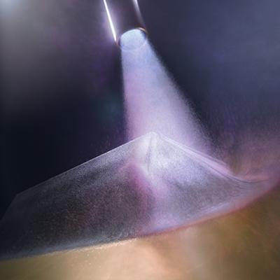
Versatile Cold Spray (VCS) enables deposition of brittle materials, such as thermoelectrics, magnets, and insulators, while retaining their functional properties. Materials can be deposited on substrates or arbitrary shapes with no requirement to match compositions. The VCS system is low cost, easily portable, and easy to use.
VCS has been developed in a collaboration between Lawrence Livermore…
Image
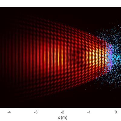
LLNL pioneered the use of tomographic reconstruction to determine the power density of electron beams using profiles of the beam taken at a number of angles. LLNL’s earlier diagnostic consisted of a fixed number of radially oriented sensor slits and required the beam to be circled over them at a fixed known diameter to collect data. The new sensor design incorporates annular slits instead,…
Image

The Optical Transconductance Varistor (OTV, formerly Opticondistor) overcomes depletion region voltage limitations by optically exciting wide bandgap materials in a compact package. A 100μm thick crystal could have the capability approaching 40kV and would replace numerous equivalent junction devices. Thus, unlike present junction transistors or diodes, this wide bandgap device can be stacked…
Image

LLNL has developed a compact and low-power cantilever-based sensor array, which has been used to detect various vapor-phase analytes. For further information on the latest developments, see the article "Sniffing the Air with an Electronic Nose."