Image
Fabrication of height modulated and tapered features in fused silica

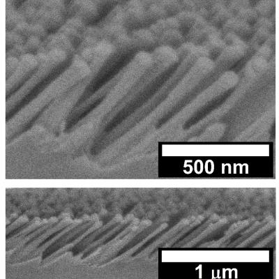
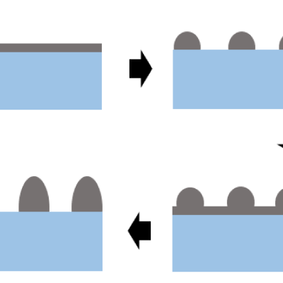
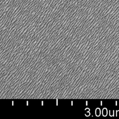
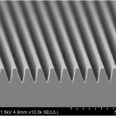
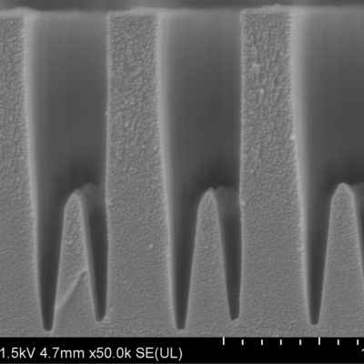
This LLNL invention allows for the fabrication of complex waveplate features and topologies from fused silica, a highly desirable and durable waveplate material.  It also is a unique technique for density multiplication and high-fidelity bidirectional deposition, which can create optical components that are generally for entirely new classes of optical materials.

Left Image Caption…

Image
Standing in LLNL’s Center for Micro Nano Technology, Nathan Ray holds a marvel of optical engineering, a 5-centimeter metasurface optic

This LLNL invention concerns a method for patterning the index of refraction by fabricating a spatially invariant metasurface, and then apply spatially varied mechanical loading to compress the metasurface features vertically and spread them radially. In doing so, the index of refraction can be re-written on the metasurface, thus enabling index patterning. This process allows rapid 'rewriting…

Image
structures created using method for producing laser gain media by atomic layer deposition

Powder atomic layer deposition process is used to coat nanopowders of host materials (e.g. yttrium aluminum garnet) with optically active neodymium organometal precursor followed by O2/O3 RF plasma to convert to a single layer of Nd2O3. The process can be repeated to build arbitrarily thick layers with custom doping profiles and followed by post-…

Image
SEM image of etched metasurface with angled features

This novel invention specifically enables the fabrication of arbitrarily tailored birefringence characteristics in nano-structured meta-surfaces on non-birefringent substrates (e.g. fused silica). The birefringent nano-structured meta-surface is produced by angled directional reactive ion beam etching through a nano-particle mask. This method enables the simultaneous tailoring of refractive…

Image
Schematic of one methodology for achieving a thicker substrate engraved meta-surface (SEMS) layer

This invention (US Patent No. 11,294,103) is an extension of another LLNL invention, US Patent No. 10,612,145, which utilizes a thin sacrificial metal mask layer deposited on a dielectric substrate (e.g. fused silica) and subsequently nanostructured through a laser generated selective thermal de-wetting process.

Image
Diffuse discharge circuit breaker with latching switch

A thyristor will stay conducting until the current through the device is zero (“current zero”) or perhaps slightly negative.  LLNL’s approach is to use the opticondistor (“OTV”) to force this current zero in order to force the device into an “off” state.  By combining a light-activated thyristor with an OTV, a noise-immune, high efficiency, high-power switching device can be…

Image
Laser peening induces deep compressive stress, which significantly extends the service lifetime over any conventional treatment

This invention proposes using a pulse laser configured to generate laser pulses and a controller for controlling operation of the pulse laser. The controller is further configured to control the pulse laser to cause the pulse laser to generate at least one of the laser pulses with a spatiotemporally varying laser fluence over a duration of at least one of the laser pulses. The spatiotemporally…

Image
Scanning electron micrograph of scalable, grating-like nanoscale metal mask (line period ~35 nm)

This invention consists of a method of forming nanoscale metal lines to produce a grating-like mask with wide area coverage over the surface of a durable optical material such as fused silica. Subsequent etching processes transfer the metal mask to the underlying substrate forming a birefringent metasurface. This method enables the production of ultrathin waveplates for high power laser…

Image
Scanning electron micrograph of bulk metamaterial structures fabricated at LLNL

Heat sensitive materials such as piezoelectric and MEMS devices and assemblies, magnetic sensors, nonlinear optical crystals, laser glass or solid-state laser materials, etc. cannot be exposed to excess temperatures which in the context of this invention, means materials that cannot be exposed to temperatures greater than 50°C (122°F). LLNL’s invention describes a low-temperature method of…

Image
LLNL energy grid protection device

The approach is to leverage the fact that a momentary “load” equal to the power transmission line impedance, (Z0), during the transient can suppress its propagation.  Z(0) is typically a fixed impedance of several hundred ohms based on the geometry of most single wire transmission lines.

So, an isolated self-powered opticondistor (OTV) system may provide an ultrafast method of…

Image
Boss Circuit Breaker

LLNL’s novel approach to enable MVDC power systems to operate safely is to develop a wideband gap bulk optical semiconductor switch (WBG BOSS) circuit breaker.  For higher power, efficiency and temperature operation, vanadium-doped silicon carbide (V-doped SiC) appears to be the most promising basis for WBG BOSS circuit breaker (other dopants like aluminum, boron and nitrogen may further…

Image
Sub-device integrated with Main device of the flow battery (A) and a cross-section of the sub-device (B)

LLNL researchers has developed an approach to mitigate HER on the ‘plating’ electrode, which uses a sub-device as a rebalancing cell to restore electrolyte properties, including pH, conductivity, and capacity across the main device of the flow battery.  This sub-device, which may need to be powered externally, has three major physical components: (1) a cathode electrode, (2) an anode…

Image
Electrical grid

LLNL has developed a novel methodology for using commercially available automated sensors and actuators which can be deployed at scale in large appliances and plug-in EVs to provide as needed electric grid stabilization capabilities. The approach comprises of a population of voltage relays with a range of setpoints that would gradually reduce load as voltage falls. More severe voltage…

Image
Electrodeposition of Zn onto 3D printed copper nanowire (CuNW)

Improving the active material of the Zn anode is critical to improving the practicality of Zn-MnO2 battery technology. LLNL researchers have developed a new category of 3D structured Zn anode using a direct-ink writing (DIW) printing process to create innovative hierarchical architectures.  The DIW ink, which is a gel-based mixture composed of zinc metal powder and organic binders, is…

Image
Compared with conventional slurry-based film electrode manufacturing methods, dry laser powder bed fusion is promising in generating structured electrodes for high power, low cost lithium ion batteries

To address many of the aforementioned challenges of manufacturing LIBs and SSBs, LLNL researchers have developed a number of inventions that offer proposed solutions for their components:

Image
Linearly polarized light entering a half-wave plate can be resolved into two waves, parallel and perpendicular to the optic axis of the waveplate ("Waveplate" by Bob Mellish is licensed under CC BY-SA 3.0).

This novel method of producing waveplates from isotropic optical materials (e.g. fused silica) consists of forming a void-dash metasurface using the following process steps:

Image
creation of ultra-high energy density matter by an intense laser pulse
Livermore Lab researchers have developed two new methods for improving the efficiency of laser drilling. The first method is based on multi-pulse laser technology. Two synchronized free-running laser pulses from a tandem-head Nd:YAG laser and a gated CW laser are capable of drilling through 1/8-in-thick stainless-steel targets at a standoff distance of 1 m without gas-assist. The combination of a…
Image
nuclear reactor

The new LLNL technique works by transiently removing and trapping concrete or rock surface material, so that contaminants are confined in a manner that is easy to isolate and remove. Our studies suggest that 10 m2 of surface could be processed per hour. The technique easily scales to more surface/hr.