

The approach is to use appropriately doped semi-insulating gallium nitride to provide a high damage tolerant photoconductor with high responsivity to various pump wavelength light. Mn, C, or Fe are used as dopants to provide a source of electrons or holes that can be excited. This is combined with the use of dichroic antireflection coating at the GaN/polyimide/liquid crystal…
Image
This LLNL invention allows for the fabrication of complex waveplate features and topologies from fused silica, a highly desirable and durable waveplate material. It also is a unique technique for density multiplication and high-fidelity bidirectional deposition, which can create optical components that are generally for entirely new classes of optical materials.
Left Image Caption…
Image
This LLNL invention concerns a method for patterning the index of refraction by fabricating a spatially invariant metasurface, and then apply spatially varied mechanical loading to compress the metasurface features vertically and spread them radially. In doing so, the index of refraction can be re-written on the metasurface, thus enabling index patterning. This process allows rapid 'rewriting…
Image
LLNL’s Distributed Implicit Neural Representation (DINR) is a novel approach to 4D time-space reconstruction of dynamic objects. DINR is the first technology to enable 4D imaging of dynamic objects at sufficiently high spatial and temporal resolutions that are necessary for real world medical and industrial applications.
Image
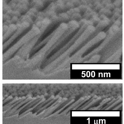
This novel invention specifically enables the fabrication of arbitrarily tailored birefringence characteristics in nano-structured meta-surfaces on non-birefringent substrates (e.g. fused silica). The birefringent nano-structured meta-surface is produced by angled directional reactive ion beam etching through a nano-particle mask. This method enables the simultaneous tailoring of refractive…
Image
This invention (US Patent No. 11,294,103) is an extension of another LLNL invention, US Patent No. 10,612,145, which utilizes a thin sacrificial metal mask layer deposited on a dielectric substrate (e.g. fused silica) and subsequently nanostructured through a laser generated selective thermal de-wetting process.
Image
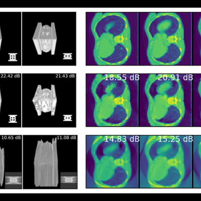
The essence of this invention is a method that couples network architecture using neural implicit representations coupled with a novel parametric motion field to perform limited angle 4D-CT reconstruction of deforming scenes.
Image

LLNL researchers has developed designs to augment WBG/UWBG-based OALVs to improve their power handling capability under CW operational environments. These designs include:
Image
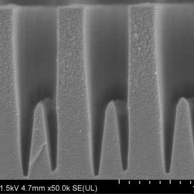
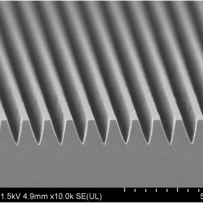
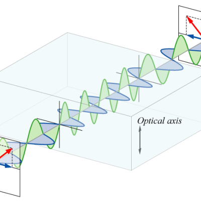
This invention consists of a method of forming nanoscale metal lines to produce a grating-like mask with wide area coverage over the surface of a durable optical material such as fused silica. Subsequent etching processes transfer the metal mask to the underlying substrate forming a birefringent metasurface. This method enables the production of ultrathin waveplates for high power laser…
Image
Heat sensitive materials such as piezoelectric and MEMS devices and assemblies, magnetic sensors, nonlinear optical crystals, laser glass or solid-state laser materials, etc. cannot be exposed to excess temperatures which in the context of this invention, means materials that cannot be exposed to temperatures greater than 50°C (122°F). LLNL’s invention describes a low-temperature method of…
Image
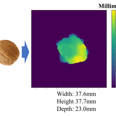
LLNL’s novel technology automates the inspection process by using a scanning system that captures data within the walnut shell without having to open the shell. The system output gives a visual image inside the walnut shell sufficient to evaluate and rate the quality of the walnut. The system uses a camara and radar that can capture data at a rapid rate. This improves speed and…
Image
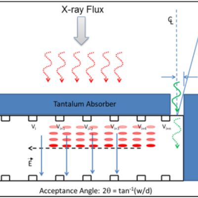
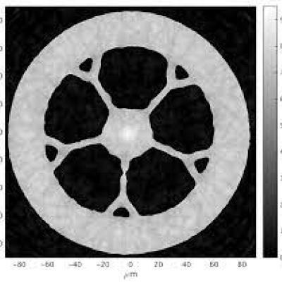
The approach is to develop a solid-state X-ray imager based on the architecture of the Silicon Drift Detector (SDD) which uses a series of cathode strips on both sides of a silicon wafer to achieve bulk depletion and electron drift. The invention leverages this SDD functionality to achieve signal stretching of liberated charge carriers from X-Ray photons that converts the time domain…
Image
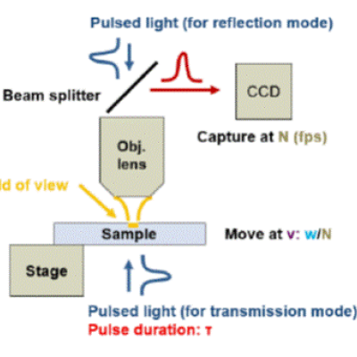
LLNL’s novel approach is to use a continuous moving camera with a scan speed of >1 mm/sec and a frame rate of 100 frames per second. The key is to have a light source that flashes with a duration of one nanosecond, thus essentially freezing the image with no blur. Clear images of high resolution can then be captured through a high-magnification objective lens (reflection mode)…
Image
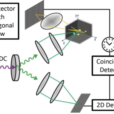
LLNL’s approach to the development of a wide-field, three-dimensional quantum (3DQ) microscope is to harness quantum entangled photons to form simultaneous 3D optical images, which could be a new paradigm for 3D volumetric imaging of biological specimens. The 3DQ microscope is comprised of a novel optical system with highly sensitive detectors and an on-demand light source of entangled…
Image
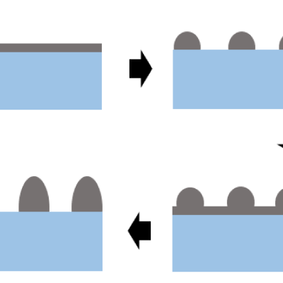
This novel method of producing waveplates from isotropic optical materials (e.g. fused silica) consists of forming a void-dash metasurface using the following process steps:
Image

Design and construction of a photoconductive switch requires a diamond photoconductor illuminated by light of a certain excitation wavelength. The diamond material is specifically doped with substitutional nitrogen, which act as a source of electrons. The device architecture allows maximum light entering the aperture. The top and bottom electrodes are made of ultra wide band…
Image

The approach is to use a custom-designed frustrum and attach it to the optical fiber that connects to the PCSS. Light from the fiber enters the frustrum, spreads out, and enters the PCSS. Any unabsorbed light re-enters the frustrum and, because of its geometry, reflects back into the PCSS itself with only a negligible fraction escaping from the fiber. The shape of the novel…
Image
To solve these challenges using new and existing CT system designs, LLNL has developed an innovative software package for CT data processing and reconstruction. Livermore Tomography Tools (LTT) is a modern integrated software package that includes all aspects of CT modeling, simulation, reconstruction, and analysis algorithms based on the latest research in the field. LTT contains the most…
Image
LLNL's 3D X-ray imager combines two different hardware pieces. The first is an x-ray optic with a depth-of-field that is small compared to the object under investigation. Reflective Wolter type x-ray optics are one such design. These hollow optics have a relatively large collection efficiency and can be designed with a large field of view. The depth of focus, which is the distance over which a…
Image

The Optical Transconductance Varistor (OTV, formerly Opticondistor) overcomes depletion region voltage limitations by optically exciting wide bandgap materials in a compact package. A 100μm thick crystal could have the capability approaching 40kV and would replace numerous equivalent junction devices. Thus, unlike present junction transistors or diodes, this wide bandgap device can be stacked…
Image
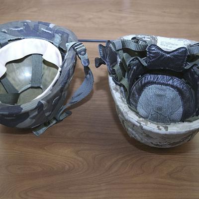
LLNL's high fidelity hydrocode is capable of predicting blast loads and directly coupling those loads to structures to predict a mechanical response. By combining this code and our expertise in modeling blast-structure interaction and damage, along with our access to experimental data and testing facilities, we can contribute to the design of protective equipment that can better mitigate the…