Rapid monolith development at scale is achieved through use of a functionally equivalent optic simulant made from a low-cost material to substitute the functional optic. Monolith optical performance is affected not only by thermal expansion but also by temperature inhomogeneity due to the temperature dependence of refractive index.
Image
Aeroptics are a proposed new class of monolithic optical system in aerogel fabricated by molding around a master mandrel. This approach combines the intrinsic stability of proven monolithic telescopes, with the ultralow density of silica aerogels. In Aeroptics, the monolith is hollow with an aerogel substrate providing a supporting structure. Theoretically, Aeroptics could enable 1-m aperture…
Image
This invention achieves both a wider field of view and faster f-number within a monolithic substrate by incorporating an aspheric convex refractive first surface and a planar aspheric field corrector surface on the final refractive surface. These two refractive surfaces work in conjunction with a concave aspheric primary and convex aspheric secondary mirror (e.g. Cassegrain type) to improve…
Image

The approach is to leverage the fact that a momentary “load” equal to the power transmission line impedance, (Z0), during the transient can suppress its propagation. Z(0) is typically a fixed impedance of several hundred ohms based on the geometry of most single wire transmission lines.
So, an isolated self-powered opticondistor (OTV) system may provide an ultrafast method of…
Image

LLNL’s novel approach is to use diamond substrates with the desired donor (nitrogen) and acceptor (boron) impurities. In order to optically activate these deep impurities, the invention requires at least one externally or internally integrated light source. The initial exposure to light can set up the desired conduction current, after which the light source could be turned off. Even with…
Image

Instead of producing individual DSRDs and bonding them, Tunnel DSRD's entire stack structure is grown epitaxially on a n- or p-type silicon wafer, resulting in a novel, “monolithic” stacked DSRD. A tunnel diode is essentially a diode with very highly doped p and n regions such that the reverse breakdown voltage is 200 meV or lower.
Image

For this method, a Silicon on Insulator (SOI) wafer is used to tailor etch rates and thickness in initial steps of the process. The simple three step process approach is comprised of grayscale lithography, deep reactive-ion etch (DRIE) and liftoff of the SOI wafer. The liftoff process is used to dissolve the insulating layer, thus separating sections of the wafer as individual silicon…
Image

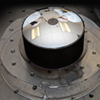
Monolithic Telescopes are a novel implementation of a solid catadioptric design form, instantiated in a monolithic block of fused silica.
Image

LLNL has developed a compact and low-power cantilever-based sensor array, which has been used to detect various vapor-phase analytes. For further information on the latest developments, see the article "Sniffing the Air with an Electronic Nose."
Image
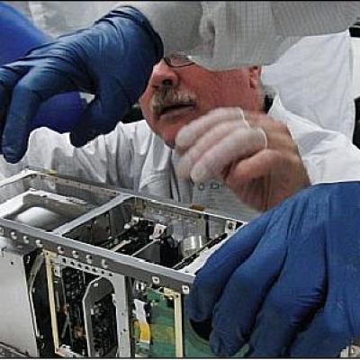
LLNL is developing the Space-based Telescopes for Actionable Refinement of Ephemeris (STARE). STARE is a constellation of low cost nano-satellites (less than 5Kg) in low-earth orbit dedicated to the observation of space debris in conjunction with a ground-based infrastructure for maintenance, coordination and data processing. Each nano-satellite in the constellation is capable of recording an…