LLNL’s invention is a photopolymerizable polymer resin that consists of one or more nitrile-functional based polymers. The resin is formulated for SLA based 3D printing allowing for the production of nitrile-containing polymer components that can then be thermally processed into a conductive, highly graphitic materials. The novelty of the invention lies in (1) the photo-curable nitrile-…
Image

Image
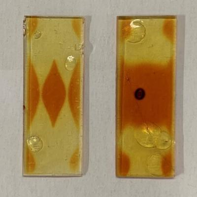
LLNL researchers have developed an innovative and uniform single-pot polymer multi-material system, based on a combination of 3 different reactive chemistries. By combining the three different constituent monomers, fine control of mechanical attributes, such as elastic modulus, can be achieved by adjusting the dosage of UV light throughout the additive manufacturing process. This results in…
Image

LLNL researchers have invented an ultrafast PCSS to drive a high-power laser diode with arbitrary pulse widths. These devices operate by supplying a high voltage (>10 kV) to one side of the switch. A short pulse of light illuminates the semiconductor, instantly turning it from highly resistive to highly conductive.
Image

LLNL’s novel approach is to use diamond substrates with the desired donor (nitrogen) and acceptor (boron) impurities. In order to optically activate these deep impurities, the invention requires at least one externally or internally integrated light source. The initial exposure to light can set up the desired conduction current, after which the light source could be turned off. Even with…
Image

Instead of producing individual DSRDs and bonding them, Tunnel DSRD's entire stack structure is grown epitaxially on a n- or p-type silicon wafer, resulting in a novel, “monolithic” stacked DSRD. A tunnel diode is essentially a diode with very highly doped p and n regions such that the reverse breakdown voltage is 200 meV or lower.
Image
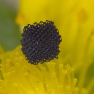
To overcome challenges that existing techniques for creating 3DGs face, LLNL researchers have developed a method that uses a light-based 3D printing process to rapidly create 3DG lattices of essentially any desired structure with graphene strut microstructure having pore sizes on the order of 10 nm. This flexible technique enables printing 3D micro-architected graphene objects with complex,…
Image

For cooling a high power device, the novel approach is to use a thermoelectric cooler (TEC)-based embedded substrate with proper selection of the TEC material as an active cooler. The packaging configuration of TEC allows cooling the entire die without the use of a fluid. The process is compatible with the thin film TEC material. Standard semiconductor processes can be used to manufacture…
Image

For this method, a Silicon on Insulator (SOI) wafer is used to tailor etch rates and thickness in initial steps of the process. The simple three step process approach is comprised of grayscale lithography, deep reactive-ion etch (DRIE) and liftoff of the SOI wafer. The liftoff process is used to dissolve the insulating layer, thus separating sections of the wafer as individual silicon…
Image

The approach is to use Charge Balance Layers (CBLs) to create a superjunction device in wide bandgap materials. These CBLs enable the device to effectively spread the electric field over 2- or 3-dimensions within a semiconductor voltage sustaining layer instead of 1-dimension, thereby increasing the maximum voltage a device is capable of withstanding. The challenge of using CBLs is the…
Image

LLNL researchers have designed and tested performance characteristics for a multichannel pyrometer that works in the NIR from 1200 to 2000 nm. A single datapoint without averaging can be acquired in 14 microseconds (sampling rate of 70,000/s). In conjunction with a diamond anvil cell, the system still works down to about 830K.
Image

By combining 3D printing and dealloying., researchers at LLNL have developed a method for fabricating metal foams with engineered hierarchical architectures consisting of pores at least 3 distinct length scales. LLNL’s method uses direct ink writing (DIW), a 3D printing technique for additive manufacturing to fabricate hierarchical nanoporous metal foams with deterministically controlled 3D…