
LLNL researchers have designed and developed a novel high-density, high-channel count 3D connector that enables hundreds or thousands of nonpermanent connections within a compact footprint. The connector addresses limitations of currently used conventional approaches that were described previously, which have an artificial ceiling on the number of recording sites of modern devices of no more…
Image
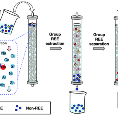
As an important step toward overcoming the technical and environmental limitations of current REE processing methods, the LLNL team has patented and demonstrated a biobased, all-aqueous REE extraction and separation scheme using the REE-selective lanmodulin protein. Lanmodulin can be fixed onto porous support materials using thiol-maleimide chemistry, which can enable tandem REE purification…
Image
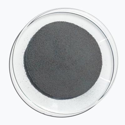
LLNL researchers have developed a Li-Sn-Zn ternary alloy and its method of production. Instead of traditional alloying techniques, the alloy was synthesized using mechanical alloying (high energy ball milling). With high purity elemental powders of lithium, tin and zinc, LLNL researchers were able to prepare Li60Sn20Zn20 as well as Li70Sn20Zn10 nanopowders.
Image

The approach is to leverage the fact that a momentary “load” equal to the power transmission line impedance, (Z0), during the transient can suppress its propagation. Z(0) is typically a fixed impedance of several hundred ohms based on the geometry of most single wire transmission lines.
So, an isolated self-powered opticondistor (OTV) system may provide an ultrafast method of…
Image

LLNL’s novel approach is to use diamond substrates with the desired donor (nitrogen) and acceptor (boron) impurities. In order to optically activate these deep impurities, the invention requires at least one externally or internally integrated light source. The initial exposure to light can set up the desired conduction current, after which the light source could be turned off. Even with…
Image

Instead of producing individual DSRDs and bonding them, Tunnel DSRD's entire stack structure is grown epitaxially on a n- or p-type silicon wafer, resulting in a novel, “monolithic” stacked DSRD. A tunnel diode is essentially a diode with very highly doped p and n regions such that the reverse breakdown voltage is 200 meV or lower.
Image

CMI—a DOE Energy Innovation Hub—is a public/private partnership led by the Ames Laboratory that brings together the best and brightest research minds from universities, national laboratories (including LLNL), and the private sector to find innovative technology solutions to make better use of materials critical to the success of clean energy technologies as well as develop resilient and secure…
Image
Many of the disadvantages of current interface devices can be overcome with LLNL’s novel interface design, which relies on area array distribution where independent interface connector subassemblies are positioned in a planar grid. Not only is the interface device expandable area-wise (without increasing contact force), but it could also be expanded height-wise, with multiple layers of these…
Image
Commercial fiber optic cables are the current standard for carrying optical signals in industries like communications or medical devices. However, the fibers are made of glass, which do not have favorable characteristics for applications that require flexibility and re-routing, e.g. typically brittle, limited selection of materials, dimension constraints.
Image
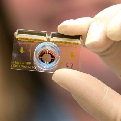
LLNL has developed a brain-on-a-chip system with a removable cell-seeding funnel to simultaneously localize neurons from various brain regions in an anatomically relevant manner and over specific electrode regions of a MEA. LLNL’s novel, removable cell seeding funnel uses a combination of 3D printing and microfabrication that allows neurons from select brain regions to easily be seeded into…