

LLNL developed a novel SOS diode structure starting with a n-type silicon wafer. On the appropriate sides of the wafer, donor and acceptor dopants with specifically designed and optimized concentration profiles are diffused in the structure. Crucially, an extra n-region is introduced to the structure to address pre-pulses. The result is a SOS diode with an optimized p+/p/n-…
Image

The approach is to use appropriately doped semi-insulating gallium nitride to provide a high damage tolerant photoconductor with high responsivity to various pump wavelength light. Mn, C, or Fe are used as dopants to provide a source of electrons or holes that can be excited. This is combined with the use of dichroic antireflection coating at the GaN/polyimide/liquid crystal…
Image

LLNL researchers have developed a TDLAS-based, standalone, real-time gas analyzer in a small form-factor for continuous or single-point monitoring. The system can analyze multiple gases with ultra-high sensitivity (ppm detection levels) in harsh conditions when utilizing wavelength-modulation spectroscopy (WMS).
Image

LLNL researchers has developed designs to augment WBG/UWBG-based OALVs to improve their power handling capability under CW operational environments. These designs include:
Image

LLNL researchers have invented an ultrafast PCSS to drive a high-power laser diode with arbitrary pulse widths. These devices operate by supplying a high voltage (>10 kV) to one side of the switch. A short pulse of light illuminates the semiconductor, instantly turning it from highly resistive to highly conductive. Ultrawide bandgap (UWBG) semiconductors are used to achieve sub-…
Image

LLNL’s novel approach is to use diamond substrates with the desired donor (nitrogen) and acceptor (boron) impurities. In order to optically activate these deep impurities, the invention requires at least one externally or internally integrated light source. The initial exposure to light can set up the desired conduction current, after which the light source could be turned…
Image

Instead of producing individual DSRDs and bonding them, Tunnel DSRD's entire stack structure is grown epitaxially on a n- or p-type silicon wafer, resulting in a novel, “monolithic” stacked DSRD. A tunnel diode is essentially a diode with very highly doped p and n regions such that the reverse breakdown voltage is 200 meV or lower.
Image

This novel detector for characterizing IFE implosions is an alternative to the current RTNADs to measure neutron fluxes > 3x10¹¹ neutrons/cm2 at high shot rates. The detector consists of a stack of small square metal wafers separated by thin insulating spacers. Every other wafer is held at high voltage while the remaining wafers are grounded. The stack acts as an…
Image

For cooling a high power device, the novel approach is to use a thermoelectric cooler (TEC)-based embedded substrate with proper selection of the TEC material as an active cooler. The packaging configuration of TEC allows cooling the entire die without the use of a fluid. The process is compatible with the thin film TEC material. Standard semiconductor processes can be used…
Image

For this method, a Silicon on Insulator (SOI) wafer is used to tailor etch rates and thickness in initial steps of the process. The simple three step process approach is comprised of grayscale lithography, deep reactive-ion etch (DRIE) and liftoff of the SOI wafer. The liftoff process is used to dissolve the insulating layer, thus separating sections of the wafer as individual…
Image

The approach is to use Charge Balance Layers (CBLs) to create a superjunction device in wide bandgap materials. These CBLs enable the device to effectively spread the electric field over 2- or 3-dimensions within a semiconductor voltage sustaining layer instead of 1-dimension, thereby increasing the maximum voltage a device is capable of withstanding. The challenge of using CBLs is…
Image

Design and construction of a photoconductive switch requires a diamond photoconductor illuminated by light of a certain excitation wavelength. The diamond material is specifically doped with substitutional nitrogen, which act as a source of electrons. The device architecture allows maximum light entering the aperture. The top and bottom electrodes are made of ultra wide band…
Image

The approach is to use a custom-designed frustrum and attach it to the optical fiber that connects to the PCSS. Light from the fiber enters the frustrum, spreads out, and enters the PCSS. Any unabsorbed light re-enters the frustrum and, because of its geometry, reflects back into the PCSS itself with only a negligible fraction escaping from the fiber. The shape of the novel…
LLNL’s SAS technology embedded within a facility is developed to sense, detect, localize, alert, and communicate an active shooter(s) to first responders. It relies on three integrated compact sensors that detect sound, infrared light (from the muzzle blast) and vibrations emanating from a gunshot. Fusing the data from these detectors minimizes false alarms.
The key to time-reversal for an active shooter detection/tracking application is being able to estimate the space-time transfer function (Green’s function) between source-enclosure-receiver. This approach begins with the acoustic mapping of an indoor muzzle blast.
Image
LLNL's high fidelity hydrocode is capable of predicting blast loads and directly coupling those loads to structures to predict a mechanical response. By combining this code and our expertise in modeling blast-structure interaction and damage, along with our access to experimental data and testing facilities, we can contribute to the design of protective equipment that can better mitigate the…
Image

Scientists at Lawrence Livermore National Laboratory have developed a plastic that can detect neutrons, something previously thought impossible.
Livermore scientists demonstrated a plastic scintillator that can discriminate between neutrons and gamma rays with a polyvinyltoluene (PVT) polymer matrix loaded with a scintillating dye, 2,5-diphenyloxazole (PPO). They have found that…
Image
LLNL's neutron "Pillar Detector" fabrication technology uses semiconductor-based micro-structured elements as an electrical signal generation medium for the detection of neutrons. These materials in the form of semiconductor "pillars" embedded in matrix of high cross-section neutron converter materials (such as Boron) that emit charged particles upon interaction with neutrons. These charged…
Image
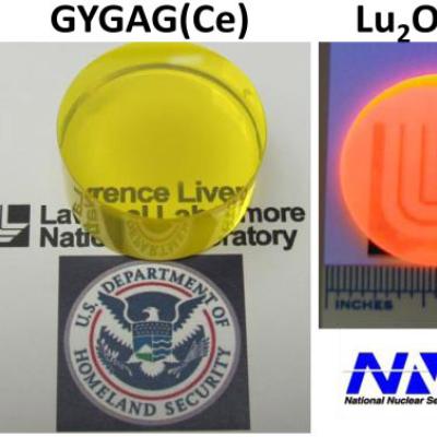
Transparent ceramic fabrication allows the production of gadolinium- , lutetium-, and terbium-based garnets which are difficult to grow by melt techniques due to phase instabilities. Phase stabilization of the garnets is accomplished by the addition of the intersubstitutional ions, Gallium and/or Scandium.
Scientists have developed many versatile and scaleable fabrication methods.…
Image

The LLNL detector measures radiation over a large dynamic range, spanning both high hazardous levels and weak levels, including natural background radiation. In weak radiation fields, the detector also measures gamma-ray spectra. The cost of the detector is significantly less than the total cost of existing separate detectors that could perform the same measurements.
Image
LLNL researchers have grown and characterized scintillator crystals of Strontium Iodide (SrI2). Scintillator energy resolution and light yield proportionality surpass NaI and are similar to LaBr3. The SrI2 scintillators doped with europium (Eu) exhibit very high light yields (> 100,000 photons/MeV), extremely good energy resolution (<3% at 662 keV) and excellent light yield…
Image

LLNL has developed a radiation detector that cools to operating temperatures in 1-2 hours using two separate cooling stages. The first cooling brings the instrument to operating temperature. The embedded second cooling system achieves portable detection that can be sustained for 8-12 hours.
In addition, an integrated, hermetically-sealed package has been developed complete with…
Image

LLNL's X-ray spectrometers based on STJ have been developed for high-resolution soft X-ray spectroscopy. STJ consist of two superconducting thin film electrodes separated by a thin insulating tunnel barrier. They measure X-ray energies from the increase in tunneling current after X-ray absorption in one of the electrodes excites additional charge carriers above the superconducting energy gap.…
Image

The Optical Transconductance Varistor (OTV, formerly Opticondistor) overcomes depletion region voltage limitations by optically exciting wide bandgap materials in a compact package. A 100μm thick crystal could have the capability approaching 40kV and would replace numerous equivalent junction devices. Thus, unlike present junction transistors or diodes, this wide bandgap device can be stacked…
Image
The invention utilizes the statistical nature of radiation transport as well as modern processing techniques to implement a physics-based, sequential statistical processor. By this we mean that instead of accumulating a pulse-height spectrum as is done in many other systems, each photon is processed individually upon arrival and then discarded. As each photon arrives, a decision is…
Image
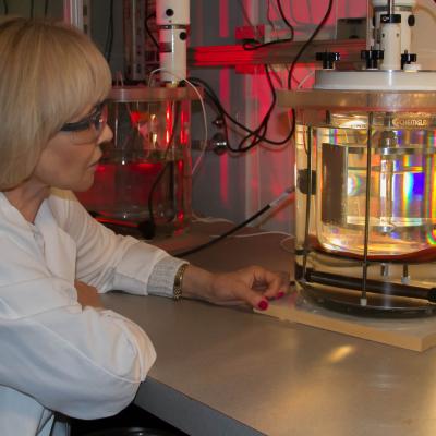
LLNL has identified solution-grown organic crystals having scintillation efficiency not only close to, but even exceeding that of stilbene.. LLNL's invention relates to a new class of neutron detectors based on scintillation response of organic single crystals. More specifically, the use of organic molecules grown from solution and to molecules including the basic benzene or phenyl structure…