
This portfolio was organized to group innovations that might not be categorized in the other portfolios. Instruments are full systems integrated to perform complex electrical or mechanical work. Sensors are devices that detect, measure, or locate a physical property. Electronics are devices that manipulate electrons or control electrical energy, and the manufacturing processes that fabricate them.
Portfolio News and Multimedia
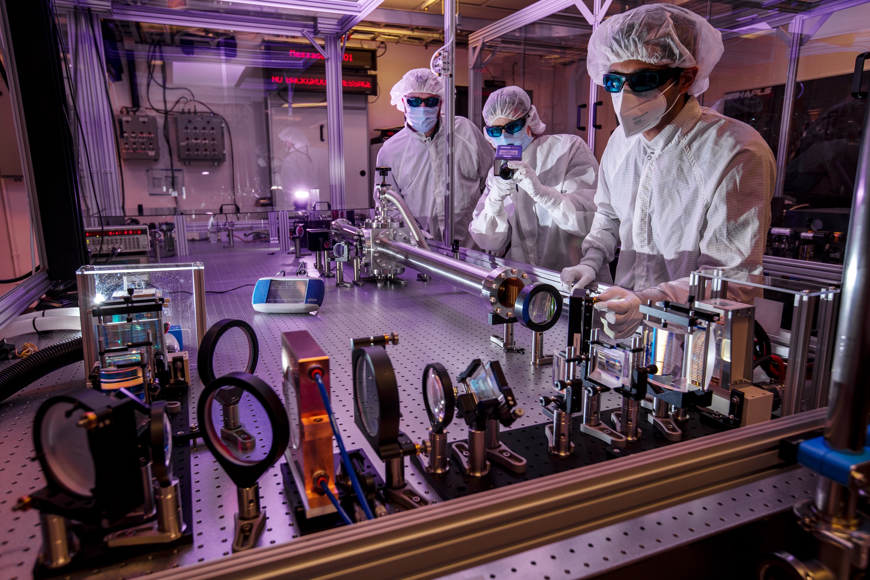
Decades of cutting-edge laser, optics and plasma physics research at Lawrence Livermore National Laboratory (LLNL) played a key role in the underlying science that the semiconductor industry uses to manufacture advanced microprocessors. Now a new research partnership led by LLNL aims to lay the groundwork for the next evolution of extreme ultraviolet (EUV) lithography, centered around a Lab-developed driver system dubbed the Big Aperture Thulium (BAT) laser.
LLNL plasma physicists, Brendan Reagan and Jackson Williams, are the project’s co-lead principal investigators. The project includes scientists from SLAC National Accelerator Laboratory; ASML San Diego; and the Advanced Research Center for Nanolithography (ARCNL), a public-private research center based in the Netherlands.
Funded through DOE’s Unlocking Lasting Transformative Resiliency Advances by Faster Actuation of power Semiconductor Technologies (ULTRAFAST) program, LLNL researchers (in Engineering) will develop an optically-controlled semiconductor transistor to enable future grid control systems to accommodate higher voltage and current than state-of-the-art devices. (Award amount: $3,000,000) while LLNL licensee Opcondys will develop a light-controlled grid protection device to suppress destructive, sudden transient surges on the grid such as those caused by lightning and electromagnetic pulses. (Award amount: $3,178,977)

The Department of Energy’s Technology Transfer Working Group recently awarded two Lawrence Livermore National Laboratory (LLNL) employees with “Best in Class” awards during their May spring meeting in Washington, D.C.

LLNL developed a novel SOS diode structure starting with a n-type silicon wafer. On the appropriate sides of the wafer, donor and acceptor dopants with specifically designed and optimized concentration profiles are diffused in the structure. Crucially, an extra n-region is introduced to the structure to address pre-pulses. The result is a SOS diode with an optimized p+/p/n-…

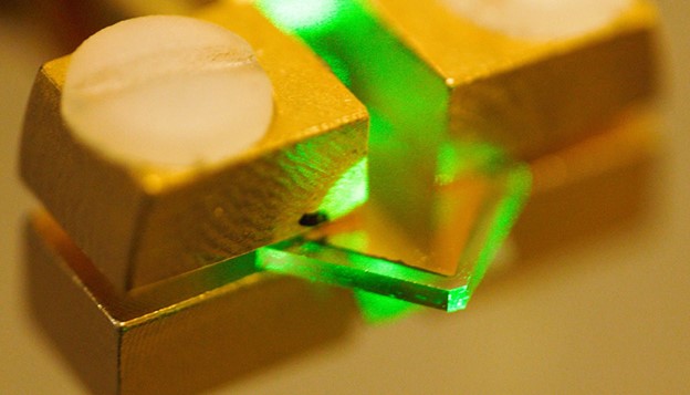
LLNL researchers have invented an ultrafast PCSS to drive a high-power laser diode with arbitrary pulse widths. These devices operate by supplying a high voltage (>10 kV) to one side of the switch. A short pulse of light illuminates the semiconductor, instantly turning it from highly resistive to highly conductive. Ultrawide bandgap (UWBG) semiconductors are used to achieve sub-…

LLNL’s novel approach is to use diamond substrates with the desired donor (nitrogen) and acceptor (boron) impurities. In order to optically activate these deep impurities, the invention requires at least one externally or internally integrated light source. The initial exposure to light can set up the desired conduction current, after which the light source could be turned…

Instead of producing individual DSRDs and bonding them, Tunnel DSRD's entire stack structure is grown epitaxially on a n- or p-type silicon wafer, resulting in a novel, “monolithic” stacked DSRD. A tunnel diode is essentially a diode with very highly doped p and n regions such that the reverse breakdown voltage is 200 meV or lower.

For cooling a high power device, the novel approach is to use a thermoelectric cooler (TEC)-based embedded substrate with proper selection of the TEC material as an active cooler. The packaging configuration of TEC allows cooling the entire die without the use of a fluid. The process is compatible with the thin film TEC material. Standard semiconductor processes can be used…

For this method, a Silicon on Insulator (SOI) wafer is used to tailor etch rates and thickness in initial steps of the process. The simple three step process approach is comprised of grayscale lithography, deep reactive-ion etch (DRIE) and liftoff of the SOI wafer. The liftoff process is used to dissolve the insulating layer, thus separating sections of the wafer as individual…

The approach is to use Charge Balance Layers (CBLs) to create a superjunction device in wide bandgap materials. These CBLs enable the device to effectively spread the electric field over 2- or 3-dimensions within a semiconductor voltage sustaining layer instead of 1-dimension, thereby increasing the maximum voltage a device is capable of withstanding. The challenge of using CBLs is…