LLNL’s invention is a photopolymerizable polymer resin that consists of one or more nitrile-functional based polymers. The resin is formulated for SLA based 3D printing allowing for the production of nitrile-containing polymer components that can then be thermally processed into a conductive, highly graphitic materials. The novelty of the invention lies in (1) the photo-curable nitrile-…
Image

Image
LLNL researchers have developed a fabrication process for creating 3D random interdigitated architectures of anodes and cathodes, eliminating the need for a membrane to separate them. This approach is similar to the repeating interdigitated multi-electrode architectures that also were developed at LLNL.
Image
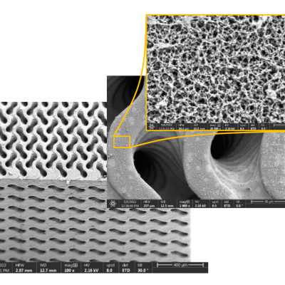
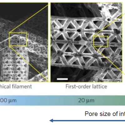
LLNL researchers have developed novel advanced manufactured biomimetic 3D-TPMS (triply periodic minimal surface) membrane architectures such as a 3D gyroid membrane. The membrane is printed using LLNL's nano-porous photoresist technology. LLNL’s 3D-TPMS membranes consist of two independent but interpenetrating macropore flow channel systems that are separated by a thin nano-porous wall. 3D-…
Image

LLNL researchers have invented an ultrafast PCSS to drive a high-power laser diode with arbitrary pulse widths. These devices operate by supplying a high voltage (>10 kV) to one side of the switch. A short pulse of light illuminates the semiconductor, instantly turning it from highly resistive to highly conductive.
Image

LLNL’s novel approach is to use diamond substrates with the desired donor (nitrogen) and acceptor (boron) impurities. In order to optically activate these deep impurities, the invention requires at least one externally or internally integrated light source. The initial exposure to light can set up the desired conduction current, after which the light source could be turned off. Even with…
Image

Instead of producing individual DSRDs and bonding them, Tunnel DSRD's entire stack structure is grown epitaxially on a n- or p-type silicon wafer, resulting in a novel, “monolithic” stacked DSRD. A tunnel diode is essentially a diode with very highly doped p and n regions such that the reverse breakdown voltage is 200 meV or lower.
Image

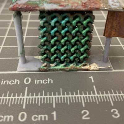
Improving the active material of the Zn anode is critical to improving the practicality of Zn-MnO2 battery technology. LLNL researchers have developed a new category of 3D structured Zn anode using a direct-ink writing (DIW) printing process to create innovative hierarchical architectures. The DIW ink, which is a gel-based mixture composed of zinc metal powder and organic binders, is extruded…
Image

CSP-POST provides the capability to inspect all incoming and outgoing emails while providing after-the-fact forensic capabilities. Using commercially available lightweight and serverless technologies, CSP-POST easily collects all email and parses it into easily searchable metadata, enriched and ready for analysis. The web-based application is deployed in a repeatable, testable, and auditable…
Image

For cooling a high power device, the novel approach is to use a thermoelectric cooler (TEC)-based embedded substrate with proper selection of the TEC material as an active cooler. The packaging configuration of TEC allows cooling the entire die without the use of a fluid. The process is compatible with the thin film TEC material. Standard semiconductor processes can be used to manufacture…
Image

LLNL has invented a new system that uses public key cryptography to differentiate between human-generated text and AI-generated text. This invention can be used to validate that text is likely to be human generated for the purposes of sorting or gatekeeping on the internet, can detect cheating on essay assignments, and can be used as an automatic captcha that does away with the hassle of…
Image
To get the best of both worlds – the sensitivity of LC-MS with the speed of PS-MS – and a functional substrate that can maintain sample integrity, LLNL researchers looked to 3D printing. They have patented a novel approach to create lattice spray substrates for direct ionization mass spectroscopy using 3D-printing processes.
Image

For this method, a Silicon on Insulator (SOI) wafer is used to tailor etch rates and thickness in initial steps of the process. The simple three step process approach is comprised of grayscale lithography, deep reactive-ion etch (DRIE) and liftoff of the SOI wafer. The liftoff process is used to dissolve the insulating layer, thus separating sections of the wafer as individual silicon…
Image

The approach is to use Charge Balance Layers (CBLs) to create a superjunction device in wide bandgap materials. These CBLs enable the device to effectively spread the electric field over 2- or 3-dimensions within a semiconductor voltage sustaining layer instead of 1-dimension, thereby increasing the maximum voltage a device is capable of withstanding. The challenge of using CBLs is the…
Image

LLNL researchers, through careful control over the chemistry, network formation, and crosslink density of the ink formulations as well as introduction of selected additives, have been successful in preparing 3D printable silicone inks with tunable material properties. For DIW (direct in writing) applications, LLNL has a growing IP portfolio around 3D printable silicone feedstocks for diverse…
Image
LLNL’s method of 3D printing fiber-reinforced composites has two enabling features:
Image

LLNL has developed a new method for securely processing protected data on HPC systems with minimal impact on the existing HPC operations and execution environment. It can be used with no alterations to traditional HPC operations and can be managed locally. It is fully compatible with traditional (unencrypted) processing and can run other jobs, unencrypted or not, on the cluster simultaneously…
Image

LLNL's NeMS system enables network mapping operations by using two LLNL-developed software systems: LLNL's NeMS tool and the Everest visualization system. Each software system can be also used separately for their specific applications. When the two systems are used together as an iterative analysis platform, LLNL's NeMS system provides network security managers and information technology…