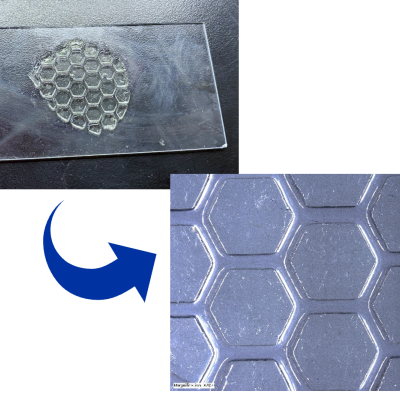
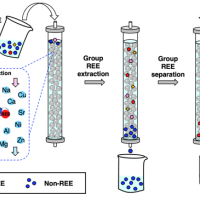
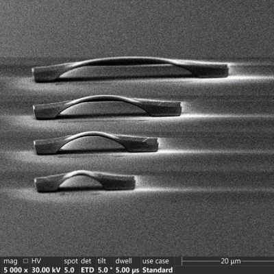
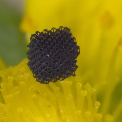
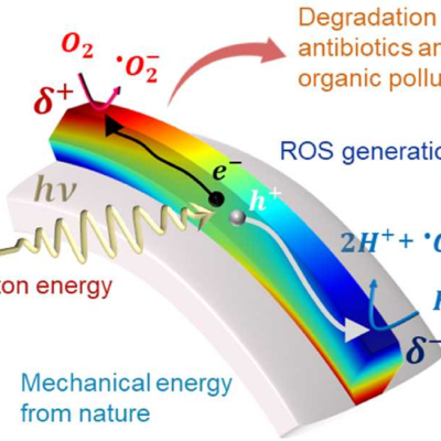
Image
Examples of different UV exposure patterns printed from the same multi-material resin.  Darker yellow regions have higher UV exposure times leading to tougher regions.

LLNL researchers have developed an innovative and uniform single-pot polymer multi-material system, based on a combination of 3 different reactive chemistries.  By combining the three different constituent monomers, fine control of mechanical attributes, such as elastic modulus, can be achieved by adjusting the dosage of UV light throughout the additive manufacturing process.  This results in…

Image
Top down view of a Gas phase synthesized graphene (GSG) UV curable polymer composite film.

LLNL researchers have developed a method to incorporate gas phase synthesized graphene (GSG) as a unique additive in a UV-crosslinkable polymer formulation. The GSG is added by using a planetary mixer to obtain a homogenous suspension of GSG in polymer. The resulting formulation is highly stable and doesn't show signs of phase separation or solid sedimentation. The polymer formulation is then…

Image
SEM image of tantalum airbridges

LLNL researchers developed a novel method to nucleate the alpha phase of Tantalum on a polymer surface at room temperature, allowing for the controllable formation of a variety of 3D structures, such as airbridges. Using this method with a subsequent Piranha etch results in the complete removal of the residues of the polymer 'scaffolding' or template while allowing the deposited tantalum…

Image
Powder in Chemical Watch Glass

LLNL researchers have developed a Li-Sn-Zn ternary alloy and its method of production.  Instead of traditional alloying techniques, the alloy was synthesized using mechanical alloying (high energy ball milling).  With high purity elemental powders of lithium, tin and zinc, LLNL researchers were able to prepare Li60Sn20Zn20 as well as Li70Sn20Zn10 nanopowders.

Image
Custom PCB design of a PCSS Laser Diode Driver

LLNL researchers have invented an ultrafast PCSS to drive a high-power laser diode with arbitrary pulse widths.  These devices operate by supplying a high voltage (>10 kV) to one side of the switch.  A short pulse of light illuminates the semiconductor, instantly turning it from highly resistive to highly conductive.

Image
JFET Device Structure

LLNL’s novel approach is to use diamond substrates with the desired donor (nitrogen) and acceptor (boron) impurities.   In order to optically activate these deep impurities, the invention requires at least one externally or internally integrated light source.  The initial exposure to light can set up the desired conduction current, after which the light source could be turned off.  Even with…

Image
Tunneling Diode between two DSRDs

Instead of producing individual DSRDs and bonding them, Tunnel DSRD's entire stack structure is grown epitaxially on a n- or p-type silicon wafer, resulting in a novel, “monolithic” stacked DSRD.  A tunnel diode is essentially a diode with very highly doped p and n regions such that the reverse breakdown voltage is 200 meV or lower. 

Image
Scanning electron microscopy image of carbonized resorcinol-formaldehyde formulation.

LLNL inventors have created innovative steps in the synthesis, carbonation and activation steps of aerogel manufacturing that allows for large scale production. These steps are:

1. Synthesis: a novel pre-cure step with subsequent gelation (RF precursor solution is heated with stirring to achieve a mixed liquid intermediate temperature, the precursor solution is then allowed to cool,…

Image
Livermore researchers support efforts to limit the need for rare-earth elements in U.S. clean-energy technologies.

CMI—a DOE Energy Innovation Hub—is a public/private partnership led by the Ames Laboratory that brings together the best and brightest research minds from universities, national laboratories (including LLNL), and the private sector to find innovative technology solutions to make better use of materials critical to the success of clean energy technologies as well as develop resilient and secure…

Image
A sample of micro-architectured graphene aerogel, made from one of the lightest materials on Earth, sits atop a flower.

To overcome challenges that existing techniques for creating 3DGs face, LLNL researchers have developed a method that uses a light-based 3D printing process to rapidly create 3DG lattices of essentially any desired structure with graphene strut microstructure having pore sizes on the order of 10 nm. This flexible technique enables printing 3D micro-architected graphene objects with complex,…

Image
thermoelectric cooler (TEC) embedded substrate for cooling of high power devices

For cooling a high power device, the novel approach is to use a thermoelectric cooler (TEC)-based embedded substrate with proper selection of the TEC material as an active cooler.  The packaging configuration of TEC allows cooling the entire die without the use of a fluid.  The process is compatible with the thin film TEC material.  Standard semiconductor processes can be used to manufacture…

Image
Biosorption-based REE recovery and Sc extraction from low-grade feedstocks.

The novel technology developed at LLNL is a new, effective means of separating and concentrating Sc from lanthanides and non-REEs in unconventional, waste-derived feedstocks, thereby transforming an essentially valueless solution into valuable Sc concentrates.  The results represent an important advance in the development of an environmentally sustainable alternative to organic solvent-based…

Image
SEM image of a prototype for a neural implant shuttle etched into a non-SOI wafer. The 7:1 (Si:Photoresist) etch selectivity used here allowed for a maximum structure height of 32 μm, with up to 75 steps of 0.4 μm height each. Scale bar 100 μm.

For this method, a Silicon on Insulator (SOI) wafer is used to tailor etch rates and thickness in initial steps of the process.  The simple three step process approach is comprised of grayscale lithography, deep reactive-ion etch (DRIE) and liftoff of the SOI wafer.  The liftoff process is used to dissolve the insulating layer, thus separating sections of the wafer as individual silicon…

Image
Unique LLNL capabilities enable GaN superjunctions

The approach is to use Charge Balance Layers (CBLs) to create a superjunction device in wide bandgap materials.  These CBLs enable the device to effectively spread the electric field over 2- or 3-dimensions within a semiconductor voltage sustaining layer instead of 1-dimension, thereby increasing the maximum voltage a device is capable of withstanding.  The challenge of using CBLs is the…

Image
natural protein lanmodulin, LanM (blue) bound to three REE ions (cyan).

LLNL researchers along with collaborators at Pennsylvania State University have found that a newly discovered natural protein named Lanmodulin (LanM) could be a potential candidate for extracting REEs from ore or other sources such as coal ash as well as purifying the REE material.  Through joint research, the scientists found that LanM undergoes a large conformational change in response to…

IPO logo over a face profile with interconnected lines

LLNL researchers have developed a custom formulated extreme low viscosity reactive silicone resin base modified with a temperature dependent thixotrope along with a modified catalyst package.  The uncatalyzed composition is capable of accepting loadings of polymer microspheres sufficient to produce a cured bulk rubber that has a density as low as 0.3 g/cc, thus compatible with high-resolution…

Image
freeze_casting_porous_materials

The LLNL method is based on freeze‐casting of aerosolized and pressurized metal salt solutions and subsequent thermal processing. This method generates both porous particles with sizes down to one micron and macroscopic monoliths with nanometer scale ligaments/struts. The material's density can be controlled during the freeze‐dried stage. Compared to conventional approaches, this method…

Image
CNT Carbon Nanotube yarns support spherical

LLNL has developed a liquid-free method that increases the overall mechanical resistance of self-supported, carbon nanotube assemblies through nanoscale reinforcement by gas-phase deposition of a thermally cross-linkable polymer. Polymer-reinforcement increases the strength of CNT yarns after crosslinking. For example, a minimal amount (<200 nm) of poly-glycidyl metacrylate (PGMA) deposited…

Image
Bio-Based Shape Memory Polymer

LLNL researchers have developed a novel method of 3D printing regular microstructured architectures and subsequent complex macrostructures from additively manufactured bio-based composite thermoset shape memory polymer composite materials. This technology for 3D additively manufactured parts utilizes up to a 4 axis control DIW system for fabricating bio­ based thermally cured epoxy based SMP…

Image
composite_material

LLNL researchers have developed the hardware and chemistry to allow additive manufacturing of short carbon fibers in a thermoset polymer matrix which have a high degree of structural alignment over conventional cast or pressed short/chopped carbon fiber polymer composites.

The invention is based on the shear dispersal, alignment and concentration of fiber fraction within a resin…

Image
metallic_nanospheres

The nanosphere synthesis process works when a nanostructured substrate is heated above a critical temperature in the presence of a small amount of metal on the nanostructured surface. The metal acts as a particular type of catalyst for nanowire formation. It is periodically segregated within the nanowire in a thermodynamically well-defined process as nanowires grow. The result is…

Image
plants Lattice

Redox ion-exchange polymers ("redox-ionites") and membranes possessing cation- and anion- exchange, amphoteric, complex-forming and oxidation-reduction abilities have been developed on the basis of the biocompatible synthetic and chemically modified natural polymers. In addition, developments have been made towards methods of obtaining of water-soluble and spatially cross-linked ionites of…