
This invention proposes using a pulse laser configured to generate laser pulses and a controller for controlling operation of the pulse laser. The controller is further configured to control the pulse laser to cause the pulse laser to generate at least one of the laser pulses with a spatiotemporally varying laser fluence over a duration of at least one of the laser pulses. The spatiotemporally…
Image

LLNL researchers have invented an ultrafast PCSS to drive a high-power laser diode with arbitrary pulse widths. These devices operate by supplying a high voltage (>10 kV) to one side of the switch. A short pulse of light illuminates the semiconductor, instantly turning it from highly resistive to highly conductive.
Image

LLNL’s novel approach is to use diamond substrates with the desired donor (nitrogen) and acceptor (boron) impurities. In order to optically activate these deep impurities, the invention requires at least one externally or internally integrated light source. The initial exposure to light can set up the desired conduction current, after which the light source could be turned off. Even with…
Image

Instead of producing individual DSRDs and bonding them, Tunnel DSRD's entire stack structure is grown epitaxially on a n- or p-type silicon wafer, resulting in a novel, “monolithic” stacked DSRD. A tunnel diode is essentially a diode with very highly doped p and n regions such that the reverse breakdown voltage is 200 meV or lower.
Image

CSP-POST provides the capability to inspect all incoming and outgoing emails while providing after-the-fact forensic capabilities. Using commercially available lightweight and serverless technologies, CSP-POST easily collects all email and parses it into easily searchable metadata, enriched and ready for analysis. The web-based application is deployed in a repeatable, testable, and auditable…
Image

For cooling a high power device, the novel approach is to use a thermoelectric cooler (TEC)-based embedded substrate with proper selection of the TEC material as an active cooler. The packaging configuration of TEC allows cooling the entire die without the use of a fluid. The process is compatible with the thin film TEC material. Standard semiconductor processes can be used to manufacture…
Image
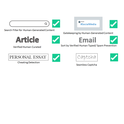
LLNL has invented a new system that uses public key cryptography to differentiate between human-generated text and AI-generated text. This invention can be used to validate that text is likely to be human generated for the purposes of sorting or gatekeeping on the internet, can detect cheating on essay assignments, and can be used as an automatic captcha that does away with the hassle of…
Image

For this method, a Silicon on Insulator (SOI) wafer is used to tailor etch rates and thickness in initial steps of the process. The simple three step process approach is comprised of grayscale lithography, deep reactive-ion etch (DRIE) and liftoff of the SOI wafer. The liftoff process is used to dissolve the insulating layer, thus separating sections of the wafer as individual silicon…
Image

The approach is to use Charge Balance Layers (CBLs) to create a superjunction device in wide bandgap materials. These CBLs enable the device to effectively spread the electric field over 2- or 3-dimensions within a semiconductor voltage sustaining layer instead of 1-dimension, thereby increasing the maximum voltage a device is capable of withstanding. The challenge of using CBLs is the…
Image

Livermore Lab researchers have developed two new methods for improving the efficiency of laser drilling. The first method is based on multi-pulse laser technology. Two synchronized free-running laser pulses from a tandem-head Nd:YAG laser and a gated CW laser are capable of drilling through 1/8-in-thick stainless-steel targets at a standoff distance of 1 m without gas-assist. The combination of a…
Image

LLNL has developed a new method for securely processing protected data on HPC systems with minimal impact on the existing HPC operations and execution environment. It can be used with no alterations to traditional HPC operations and can be managed locally. It is fully compatible with traditional (unencrypted) processing and can run other jobs, unencrypted or not, on the cluster simultaneously…
Image
LLNL’s system consists of one or more flashlamp-pumped Nd:glass zig-zag amplifiers, a very low threshold stimulated-Brillouin-scattering (SBS) phase conjugator system, and a free-running single frequency Nd:YLF master oscillator.
Image

The new LLNL technique works by transiently removing and trapping concrete or rock surface material, so that contaminants are confined in a manner that is easy to isolate and remove. Our studies suggest that 10 m2 of surface could be processed per hour. The technique easily scales to more surface/hr.
Image
LLNL's NeMS system enables network mapping operations by using two LLNL-developed software systems: LLNL's NeMS tool and the Everest visualization system. Each software system can be also used separately for their specific applications. When the two systems are used together as an iterative analysis platform, LLNL's NeMS system provides network security managers and information technology…