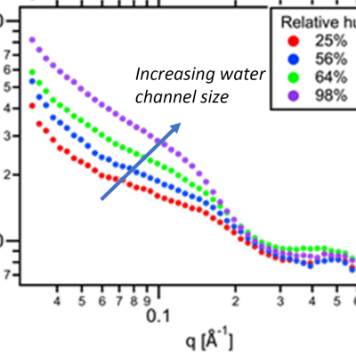
LLNL researchers have developed a method to enhance the performance of polyelectrolyte membranes by using a humidity-controlled crosslinking process which can be applied to precisely adjust the water channels of the membrane.
Image
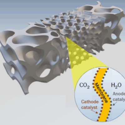
LLNL’s researchers use physical vapor deposition (sputter deposition or electron beam deposition) to coat an inert gasket material (i.e. PTFE) with a conductive metal (i.e. copper). The gas diffusion electrode overlaps onto the copper coated gasket to allow for electrical conductivity between the catalyst surface and the flow field/current collector of a CO2 electrolyzer. The coated gasket…
Image
Using their computational design optimization, LLNL researchers have developed copper-based dilute alloy catalysts (contains <10 at.% of the minority metal alloy component) and demonstrated these novel catalysts have improved energy efficiency and selectivity of the methane conversion reaction. By alloying copper with a small amount of the electropositive minority metal element, the…
Image

LLNL researchers have invented an ultrafast PCSS to drive a high-power laser diode with arbitrary pulse widths. These devices operate by supplying a high voltage (>10 kV) to one side of the switch. A short pulse of light illuminates the semiconductor, instantly turning it from highly resistive to highly conductive.
Image

LLNL’s novel approach is to use diamond substrates with the desired donor (nitrogen) and acceptor (boron) impurities. In order to optically activate these deep impurities, the invention requires at least one externally or internally integrated light source. The initial exposure to light can set up the desired conduction current, after which the light source could be turned off. Even with…
Image

Instead of producing individual DSRDs and bonding them, Tunnel DSRD's entire stack structure is grown epitaxially on a n- or p-type silicon wafer, resulting in a novel, “monolithic” stacked DSRD. A tunnel diode is essentially a diode with very highly doped p and n regions such that the reverse breakdown voltage is 200 meV or lower.
Image
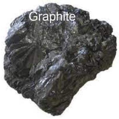
LLNL’s innovation offers an alternate synthetic route to graphite at lower cost using a molten salt mixture of CaCl2-CaCO3-CaO. The synthetic production of graphite and other high-value carbon materials is accomplished in molten salt media via electrochemical reduction and transformation of the carbon from the carbonate ion. The broad electrochemical window of molten salts enables the…
Image
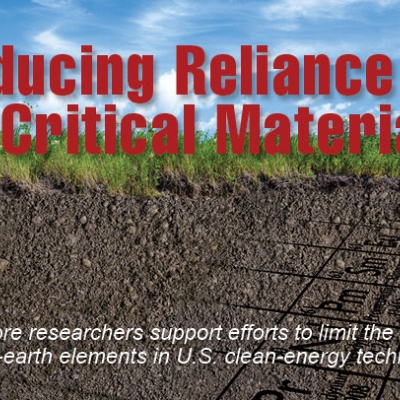
CMI—a DOE Energy Innovation Hub—is a public/private partnership led by the Ames Laboratory that brings together the best and brightest research minds from universities, national laboratories (including LLNL), and the private sector to find innovative technology solutions to make better use of materials critical to the success of clean energy technologies as well as develop resilient and secure…
Image
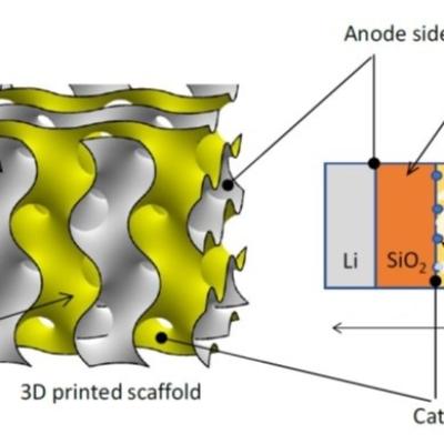
LLNL researchers have developed a new 3D printable lithium-air battery that uses a novel thin solid state ceramic electrolyte. LLNL’s invention overcomes the combined challenges of low power density and low cycle life in previously designed lithium-air batteries by using solid state electrolytes to achieve stability and multiscale structuring of the electrolyte to achieve low interfacial…
Image

For cooling a high power device, the novel approach is to use a thermoelectric cooler (TEC)-based embedded substrate with proper selection of the TEC material as an active cooler. The packaging configuration of TEC allows cooling the entire die without the use of a fluid. The process is compatible with the thin film TEC material. Standard semiconductor processes can be used to manufacture…
Image

For this method, a Silicon on Insulator (SOI) wafer is used to tailor etch rates and thickness in initial steps of the process. The simple three step process approach is comprised of grayscale lithography, deep reactive-ion etch (DRIE) and liftoff of the SOI wafer. The liftoff process is used to dissolve the insulating layer, thus separating sections of the wafer as individual silicon…
Image

The approach is to use Charge Balance Layers (CBLs) to create a superjunction device in wide bandgap materials. These CBLs enable the device to effectively spread the electric field over 2- or 3-dimensions within a semiconductor voltage sustaining layer instead of 1-dimension, thereby increasing the maximum voltage a device is capable of withstanding. The challenge of using CBLs is the…
Image
The novel LLNL approach is to use projection microstereolithography (LAPµSL), starting with a photocurable methacrylate resin formulation consisting of a combination of a photoinitiator, photoabsorber, inhibitor, solvents, and other additives. Prior to use, the resin is pretreated to control viscosity for easier handling. The resin is fed to a LAPµSL printer which employs a near UV light…
Image
The inventors have developed a 3% Yttria partially-stabilized Zirconia (3YZ) ceramic ink that produces parts with both nano and microporosity and is compatible with two AM techniques: DIW and projection microstereolithography (PμSL). The 3YZ nano-porous ceramic printed parts had engineered macro cavities measuring several millimeters in length, wall thicknesses ranging from 200 to 540 μm, and…
Image
This invention describes a multiple nozzle microfluidic unit that allows simultaneous generation streams of multiple layered coaxial liquid jets. Liquids are pumped into the device at a combined flow rate from 100 mL/hr to 10 L/hr. Droplets are created with diameters in the range of 1 µm to 5 mm and can be created with 1-2 shell layers encapsulating fluid. Droplets created from the system can…
Image

Livermore researchers have developed two novel TiCl4 based non-alkoxide sol-gel approaches for the synthesis of SiO2/TiO2 nanocomposite aerogels. Composite SiO2-TiO2 aerogels were obtained by epoxide-assisted gelation (EAG route) of TiCl4/DMF solution in the presence SiO2 aerogel particles. Additionally, the same TiCl4/DMF solution was employed to prepare SiO2@TiO2 aerogels by a facile one-…
Image

Nanomaterials that are emerging out of cutting edge nanotechnology research are a key component for an energy revolution. Carbon-based nanomaterials are ushering in the "new carbon age" with carbon nanotubes, nanoporous carbons, and graphene nanosheets that will prove necessary to provide sustainable energy applications that lessen our dependence on fossil fuels.
Carbon aerogels (CAs)…
Image

Chemical and biological sensors based on nanowire or nanotube technologies exhibit observable ultrasensitive detection limits due to their unusually large surface-to-volume architecture. This suggests that nanosensors can provide a distinct advantage over conventional designs. This advantage is further enhanced when the nanosensor can harvest its meager power requirements from the surrounding…
Image
LLNL has developed novel nanoporous carbon materials for the surface-stress-induced actuator technology. The morphology of these materials has been designed to combine high surface area and mechanical strength. The process allows for the fabrication of large monolithic pieces with low densities and high structural integrity. One actuation technology relies on electrochemically- induced changes…