

LLNL developed a novel SOS diode structure starting with a n-type silicon wafer. On the appropriate sides of the wafer, donor and acceptor dopants with specifically designed and optimized concentration profiles are diffused in the structure. Crucially, an extra n-region is introduced to the structure to address pre-pulses. The result is a SOS diode with an optimized p+/p/n-…
Image

LLNL researchers have developed an approach to form silicon carbide (and diamond) nanoneedles using plasma etching that create micro pillars followed by chemical etching of the pillars in forming gas containing hydrogen and nitrogen. Combining these two etching processes allow for fabrication of micro- and nanoneedles that are thinner and sharper than conventionally fabricated needles.
Image

LLNL researchers have designed and developed a novel high-density, high-channel count 3D connector that enables hundreds or thousands of nonpermanent connections within a compact footprint. The connector addresses limitations of currently used conventional approaches that were described previously, which have an artificial ceiling on the number of recording sites of modern devices of no more…
Image

This invention proposes to engineer the current density along the length of a laser diode to overcome the penalty associated with non-uniformity resulting from asymmetry in the gain, photon or carrier density despite having uniform contact. Optimizing the current density profile enables diode lasers to operate with greater power conversion efficiency or operate with equivalent power conversion…
Image

This invention proposes to engineer the temperature dependence of the emission wavelength of LEDs and laser diodes. The approach is to use a strain-inducing coating to counteract the intrinsic temperature coefficient of the emission wavelength of the LED or laser diode device thereby rendering it athermal. This invention avoids additional complexity, size, weight and power dissipation of…
Image

This invention proposes a method to overcome the key limitation of electrically pumped lasers based on AlN, AlGaN, or AlInGaN, namely the lack of suitable shallow donor and acceptor dopants. As the band gap of these materials increases (and the emission wavelength decreases), both electrons and holes require greater thermal energies in order to ionize.
Image
Laser diode lensing effect can be substantially reduced by creating a pattern interface such that the substrate is only attached at the diode mesa. This is achieved by either creating a pattern solder joint and/or pattern substrate.
Image

The approach is to leverage the fact that a momentary “load” equal to the power transmission line impedance, (Z0), during the transient can suppress its propagation. Z(0) is typically a fixed impedance of several hundred ohms based on the geometry of most single wire transmission lines.
So, an isolated self-powered opticondistor (OTV) system may provide an ultrafast method of…
Image

LLNL’s novel approach is to use diamond substrates with the desired donor (nitrogen) and acceptor (boron) impurities. In order to optically activate these deep impurities, the invention requires at least one externally or internally integrated light source. The initial exposure to light can set up the desired conduction current, after which the light source could be turned…
Image

Instead of producing individual DSRDs and bonding them, Tunnel DSRD's entire stack structure is grown epitaxially on a n- or p-type silicon wafer, resulting in a novel, “monolithic” stacked DSRD. A tunnel diode is essentially a diode with very highly doped p and n regions such that the reverse breakdown voltage is 200 meV or lower.
Image
Many of the disadvantages of current interface devices can be overcome with LLNL’s novel interface design, which relies on area array distribution where independent interface connector subassemblies are positioned in a planar grid. Not only is the interface device expandable area-wise (without increasing contact force), but it could also be expanded height-wise, with multiple layers of…
Image
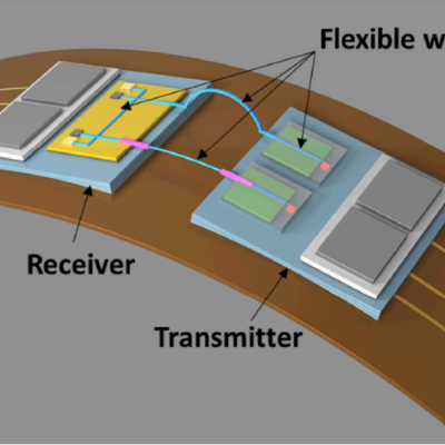
Commercial fiber optic cables are the current standard for carrying optical signals in industries like communications or medical devices. However, the fibers are made of glass, which do not have favorable characteristics for applications that require flexibility and re-routing, e.g. typically brittle, limited selection of materials, dimension constraints.
Image
LLNL has developed a brain-on-a-chip system with a removable cell-seeding funnel to simultaneously localize neurons from various brain regions in an anatomically relevant manner and over specific electrode regions of a MEA. LLNL’s novel, removable cell seeding funnel uses a combination of 3D printing and microfabrication that allows neurons from select brain regions to easily be seeded into…