

LLNL developed a novel SOS diode structure starting with a n-type silicon wafer. On the appropriate sides of the wafer, donor and acceptor dopants with specifically designed and optimized concentration profiles are diffused in the structure. Crucially, an extra n-region is introduced to the structure to address pre-pulses. The result is a SOS diode with an optimized p+/p/n-…
Image

This invention works by imaging an ultrafast pulse diffracted from a large grating onto a spatial light modulator (SLM) thereby directly transcribing an arbitrary record on a pulse front tilted (PFT) ultrafast pulse. The grating generates PFT of the input pulse, and the SLM provides temporal control of the pulse through the space-to-time mapping of the tilted pulse. Coupling this patterned…
Image
This invention exploits the non-linearities of optical Mach-Zehnder (MZ) electrooptic modulators to enhance small signal dynamic range at higher bandwidths. A linear photodiode (PD) converts the amplified optical signal output from the MZ back to an electrical signal completing an Electrical-Optical-Electrical (EOE) conversion cycle. The dynamic range can be further enhanced by daisy chaining…
Image

LLNL researchers have invented an ultrafast PCSS to drive a high-power laser diode with arbitrary pulse widths. These devices operate by supplying a high voltage (>10 kV) to one side of the switch. A short pulse of light illuminates the semiconductor, instantly turning it from highly resistive to highly conductive. Ultrawide bandgap (UWBG) semiconductors are used to achieve sub-…
Image

LLNL’s novel approach is to use diamond substrates with the desired donor (nitrogen) and acceptor (boron) impurities. In order to optically activate these deep impurities, the invention requires at least one externally or internally integrated light source. The initial exposure to light can set up the desired conduction current, after which the light source could be turned…
Image

Instead of producing individual DSRDs and bonding them, Tunnel DSRD's entire stack structure is grown epitaxially on a n- or p-type silicon wafer, resulting in a novel, “monolithic” stacked DSRD. A tunnel diode is essentially a diode with very highly doped p and n regions such that the reverse breakdown voltage is 200 meV or lower.
Image

CSP-POST provides the capability to inspect all incoming and outgoing emails while providing after-the-fact forensic capabilities. Using commercially available lightweight and serverless technologies, CSP-POST easily collects all email and parses it into easily searchable metadata, enriched and ready for analysis. The web-based application is deployed in a repeatable, testable, and auditable…
Image

For cooling a high power device, the novel approach is to use a thermoelectric cooler (TEC)-based embedded substrate with proper selection of the TEC material as an active cooler. The packaging configuration of TEC allows cooling the entire die without the use of a fluid. The process is compatible with the thin film TEC material. Standard semiconductor processes can be used…
Image

LLNL has invented a new system that uses public key cryptography to differentiate between human-generated text and AI-generated text. This invention can be used to validate that text is likely to be human generated for the purposes of sorting or gatekeeping on the internet, can detect cheating on essay assignments, and can be used as an automatic captcha that does away with the hassle of…
Image

For this method, a Silicon on Insulator (SOI) wafer is used to tailor etch rates and thickness in initial steps of the process. The simple three step process approach is comprised of grayscale lithography, deep reactive-ion etch (DRIE) and liftoff of the SOI wafer. The liftoff process is used to dissolve the insulating layer, thus separating sections of the wafer as individual…
Image

The approach is to use Charge Balance Layers (CBLs) to create a superjunction device in wide bandgap materials. These CBLs enable the device to effectively spread the electric field over 2- or 3-dimensions within a semiconductor voltage sustaining layer instead of 1-dimension, thereby increasing the maximum voltage a device is capable of withstanding. The challenge of using CBLs is…
Image
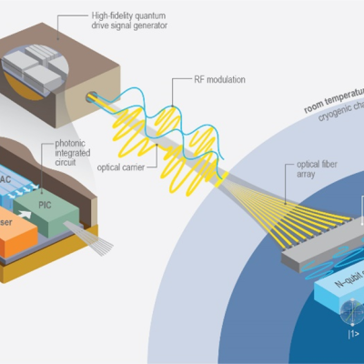
LLNL researchers in the NIF Directorate DoD Technologies RF Photonics Group explored phase modulation solutions to this signal processing challenge. Optical frequency combs offer phase noise characteristics that are orders of magnitude lower than available from commercial microwave references. The Photonics Group researchers recognized that by converting the intensity information into phase,…
Image

LLNL has developed a new method for securely processing protected data on HPC systems with minimal impact on the existing HPC operations and execution environment. It can be used with no alterations to traditional HPC operations and can be managed locally. It is fully compatible with traditional (unencrypted) processing and can run other jobs, unencrypted or not, on the cluster simultaneously…