

LLNL developed a novel SOS diode structure starting with a n-type silicon wafer. On the appropriate sides of the wafer, donor and acceptor dopants with specifically designed and optimized concentration profiles are diffused in the structure. Crucially, an extra n-region is introduced to the structure to address pre-pulses. The result is a SOS diode with an optimized p+/p/n-…
Image
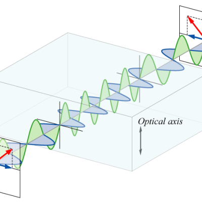
This LLNL invention allows for the fabrication of complex waveplate features and topologies from fused silica, a highly desirable and durable waveplate material. It also is a unique technique for density multiplication and high-fidelity bidirectional deposition, which can create optical components that are generally for entirely new classes of optical materials.
Left Image Caption…
Image
This LLNL invention is a wide bandgap (WBG) or ultra-wide bandgap (UWBG) material comprising a PCSS that is modified, either chemically through alloying and/or mechanically through strain fields, in order to tune the energetic positions of the valence and/or conduction bands and the associated optical transition energies that create and quench the PCSS responsivity.
Image
This LLNL invention concerns a method for patterning the index of refraction by fabricating a spatially invariant metasurface, and then apply spatially varied mechanical loading to compress the metasurface features vertically and spread them radially. In doing so, the index of refraction can be re-written on the metasurface, thus enabling index patterning. This process allows rapid 'rewriting…
Image
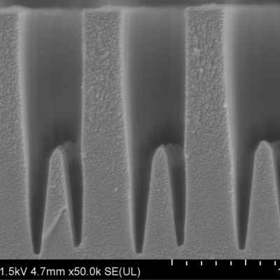
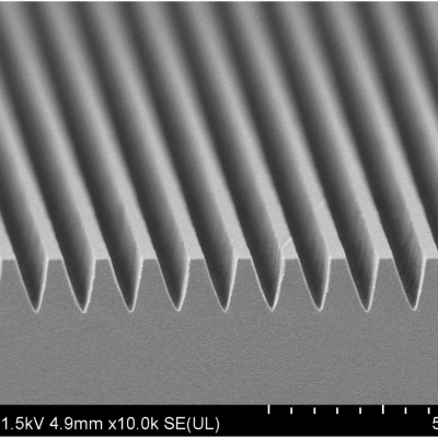
This novel invention specifically enables the fabrication of arbitrarily tailored birefringence characteristics in nano-structured meta-surfaces on non-birefringent substrates (e.g. fused silica). The birefringent nano-structured meta-surface is produced by angled directional reactive ion beam etching through a nano-particle mask. This method enables the simultaneous tailoring of refractive…
Image
This invention (US Patent No. 11,294,103) is an extension of another LLNL invention, US Patent No. 10,612,145, which utilizes a thin sacrificial metal mask layer deposited on a dielectric substrate (e.g. fused silica) and subsequently nanostructured through a laser generated selective thermal de-wetting process.
Image

A thyristor will stay conducting until the current through the device is zero (“current zero”) or perhaps slightly negative. LLNL’s approach is to use the opticondistor (“OTV”) to force this current zero in order to force the device into an “off” state. By combining a light-activated thyristor with an OTV, a noise-immune, high efficiency, high-power switching device can be…
Image

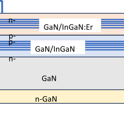
The researchers’ approach leverages the concept that dopants have high diffusivities in Ga2O3; the key lies in the selection of the appropriate dopant. This LLNL invention describes two device types that employ this design:
Image

Design and construction of a photoconductive switch requires a diamond photoconductor illuminated by light of a certain excitation wavelength.
Characteristics of the LLNL-developed switch are as follows:
Image
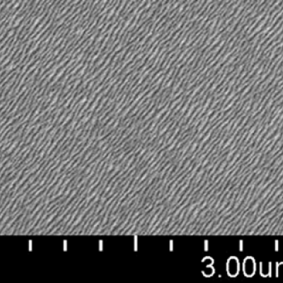
This invention consists of a method of forming nanoscale metal lines to produce a grating-like mask with wide area coverage over the surface of a durable optical material such as fused silica. Subsequent etching processes transfer the metal mask to the underlying substrate forming a birefringent metasurface. This method enables the production of ultrathin waveplates for high power laser…
Image
Heat sensitive materials such as piezoelectric and MEMS devices and assemblies, magnetic sensors, nonlinear optical crystals, laser glass or solid-state laser materials, etc. cannot be exposed to excess temperatures which in the context of this invention, means materials that cannot be exposed to temperatures greater than 50°C (122°F). LLNL’s invention describes a low-temperature method of…
Image

LLNL researchers have invented an ultrafast PCSS to drive a high-power laser diode with arbitrary pulse widths. These devices operate by supplying a high voltage (>10 kV) to one side of the switch. A short pulse of light illuminates the semiconductor, instantly turning it from highly resistive to highly conductive. Ultrawide bandgap (UWBG) semiconductors are used to achieve sub-…
Image

The approach is to leverage the fact that a momentary “load” equal to the power transmission line impedance, (Z0), during the transient can suppress its propagation. Z(0) is typically a fixed impedance of several hundred ohms based on the geometry of most single wire transmission lines.
So, an isolated self-powered opticondistor (OTV) system may provide an ultrafast method of…
Image

LLNL’s novel approach is to use diamond substrates with the desired donor (nitrogen) and acceptor (boron) impurities. In order to optically activate these deep impurities, the invention requires at least one externally or internally integrated light source. The initial exposure to light can set up the desired conduction current, after which the light source could be turned…
Image

Instead of producing individual DSRDs and bonding them, Tunnel DSRD's entire stack structure is grown epitaxially on a n- or p-type silicon wafer, resulting in a novel, “monolithic” stacked DSRD. A tunnel diode is essentially a diode with very highly doped p and n regions such that the reverse breakdown voltage is 200 meV or lower.
Image

U.S. Patent No. 11,555,965 describes LLNL’s invention of “Illumination Frustums” for photoconductive switches to capture and “frustrate” the light from leaving the frustum. LLNL researcher’s latest novel invention, “Twister Oven”, achieves this by encouraging laser light absorption in a photo conductor material. Light enters the oven twisting and reflecting, making near normal…
Image

LLNL researchers faced this challenge by bridging the gap between VEDs and solid-state electronics (SSE). Their approach was to create a hybrid vacuum microelectronic device (VMD) architecture that combines the properties of vacuum as the electronic medium and the compact form factor and manufacturing scalability of semiconductor microelectronic chips.
Image
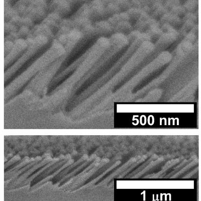
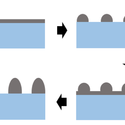
This novel method of producing waveplates from isotropic optical materials (e.g. fused silica) consists of forming a void-dash metasurface using the following process steps:
Image

Design and construction of a photoconductive switch requires a diamond photoconductor illuminated by light of a certain excitation wavelength. The diamond material is specifically doped with substitutional nitrogen, which act as a source of electrons. The device architecture allows maximum light entering the aperture. The top and bottom electrodes are made of ultra wide band…
Image

The approach is to use a custom-designed frustrum and attach it to the optical fiber that connects to the PCSS. Light from the fiber enters the frustrum, spreads out, and enters the PCSS. Any unabsorbed light re-enters the frustrum and, because of its geometry, reflects back into the PCSS itself with only a negligible fraction escaping from the fiber. The shape of the novel…