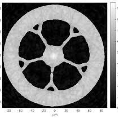
The essence of this invention is a method that couples network architecture using neural implicit representations coupled with a novel parametric motion field to perform limited angle 4D-CT reconstruction of deforming scenes.
Image

LLNL researchers have invented an ultrafast PCSS to drive a high-power laser diode with arbitrary pulse widths. These devices operate by supplying a high voltage (>10 kV) to one side of the switch. A short pulse of light illuminates the semiconductor, instantly turning it from highly resistive to highly conductive.
Image

LLNL’s novel approach is to use diamond substrates with the desired donor (nitrogen) and acceptor (boron) impurities. In order to optically activate these deep impurities, the invention requires at least one externally or internally integrated light source. The initial exposure to light can set up the desired conduction current, after which the light source could be turned off. Even with…
Image

Instead of producing individual DSRDs and bonding them, Tunnel DSRD's entire stack structure is grown epitaxially on a n- or p-type silicon wafer, resulting in a novel, “monolithic” stacked DSRD. A tunnel diode is essentially a diode with very highly doped p and n regions such that the reverse breakdown voltage is 200 meV or lower.
Image

For cooling a high power device, the novel approach is to use a thermoelectric cooler (TEC)-based embedded substrate with proper selection of the TEC material as an active cooler. The packaging configuration of TEC allows cooling the entire die without the use of a fluid. The process is compatible with the thin film TEC material. Standard semiconductor processes can be used to manufacture…
Image

For this method, a Silicon on Insulator (SOI) wafer is used to tailor etch rates and thickness in initial steps of the process. The simple three step process approach is comprised of grayscale lithography, deep reactive-ion etch (DRIE) and liftoff of the SOI wafer. The liftoff process is used to dissolve the insulating layer, thus separating sections of the wafer as individual silicon…
Image

The approach is to use Charge Balance Layers (CBLs) to create a superjunction device in wide bandgap materials. These CBLs enable the device to effectively spread the electric field over 2- or 3-dimensions within a semiconductor voltage sustaining layer instead of 1-dimension, thereby increasing the maximum voltage a device is capable of withstanding. The challenge of using CBLs is the…
Image
To solve these challenges using new and existing CT system designs, LLNL has developed an innovative software package for CT data processing and reconstruction. Livermore Tomography Tools (LTT) is a modern integrated software package that includes all aspects of CT modeling, simulation, reconstruction, and analysis algorithms based on the latest research in the field. LTT contains the most…
Image
LLNL's method of equivalent time sampling incorporates an embedded system that generates the pulses used to trigger the external circuit and the data acquisition (DAQ). This removes the external reference clock, allowing the overall system clock rate to change based on the ability of the embedded system. The time delays needed to create the time stepping for equivalent time sampling is done by…