
LLNL researchers have invented an ultrafast PCSS to drive a high-power laser diode with arbitrary pulse widths. These devices operate by supplying a high voltage (>10 kV) to one side of the switch. A short pulse of light illuminates the semiconductor, instantly turning it from highly resistive to highly conductive.
Image

LLNL’s novel approach is to use diamond substrates with the desired donor (nitrogen) and acceptor (boron) impurities. In order to optically activate these deep impurities, the invention requires at least one externally or internally integrated light source. The initial exposure to light can set up the desired conduction current, after which the light source could be turned off. Even with…
Image

Instead of producing individual DSRDs and bonding them, Tunnel DSRD's entire stack structure is grown epitaxially on a n- or p-type silicon wafer, resulting in a novel, “monolithic” stacked DSRD. A tunnel diode is essentially a diode with very highly doped p and n regions such that the reverse breakdown voltage is 200 meV or lower.
Image

A set of images generated by multiple passes over the same area can be coherently integrated by this technology developed by LLNL researchers. The primary difficulty with coherently combining different passes is registering the images obtained from each pass, particularly if a pass only partially covers a given area.
Image

For cooling a high power device, the novel approach is to use a thermoelectric cooler (TEC)-based embedded substrate with proper selection of the TEC material as an active cooler. The packaging configuration of TEC allows cooling the entire die without the use of a fluid. The process is compatible with the thin film TEC material. Standard semiconductor processes can be used to manufacture…
Image

For this method, a Silicon on Insulator (SOI) wafer is used to tailor etch rates and thickness in initial steps of the process. The simple three step process approach is comprised of grayscale lithography, deep reactive-ion etch (DRIE) and liftoff of the SOI wafer. The liftoff process is used to dissolve the insulating layer, thus separating sections of the wafer as individual silicon…
Image

The approach is to use Charge Balance Layers (CBLs) to create a superjunction device in wide bandgap materials. These CBLs enable the device to effectively spread the electric field over 2- or 3-dimensions within a semiconductor voltage sustaining layer instead of 1-dimension, thereby increasing the maximum voltage a device is capable of withstanding. The challenge of using CBLs is the…
Image
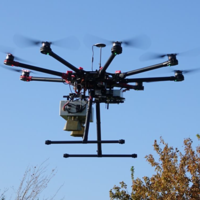
LLNL researchers have developed a lightweight drone-based GPR array that when flown over a surface with laid and/or buried objects could image the field of view and be able to detect targets and discriminate them from clutter. The imaging method employs a modified multi-static architecture to provide the highest signal to noise with the lowest system weight, making it ideal for airborne or…
Image
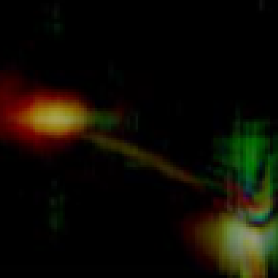
This technology uses three different frequency bands to create intensity maps of returned signals. Signals have traditionally been displayed as raw return data. The intensity of the return is represented by level of brightness. Assignment of a scalar value for intensity is used to determine the brightness of the image. In this technology, each frequency is given a designated primary color…
Image

LLNL has developed a wide band (WB) ground penetrating radar (GPR) technology to detect and image buried objects under a moving vehicle. Efficient and high performance processing algorithms reconstruct images of buried or hidden objects in two or three dimensions under a scanning array. The technology includes a mobile high-performance computing system allowing GPR array sensor data to be…